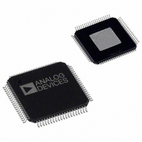
AD8384ASVZ Analog Devices Inc, AD8384ASVZ Datasheet - Page 15

AD8384ASVZ
Manufacturer Part Number
AD8384ASVZ
Description
IC DRIVER LCD 6CH 10BIT 80-TQFP
Manufacturer
Analog Devices Inc
Series
DecDriver™r
Datasheet
1.AD8384ASVZ.pdf
(24 pages)
Specifications of AD8384ASVZ
Display Type
LCD
Interface
3-Wire Serial
Current - Supply
40mA
Voltage - Supply
9 V ~ 18 V
Operating Temperature
0°C ~ 85°C
Mounting Type
Surface Mount
Package / Case
80-TQFP Exposed Pad, 80-eTQFP, 80-HTQFP, 80-VQFP
Lead Free Status / RoHS Status
Lead free / RoHS Compliant
Configuration
-
Digits Or Characters
-
Available stocks
Company
Part Number
Manufacturer
Quantity
Price
Company:
Part Number:
AD8384ASVZ
Manufacturer:
Analog Devices Inc
Quantity:
10 000
FUNCTIONAL DESCRIPTION
The AD8384 is a system building block designed to directly
drive the columns of LCD microdisplays of the type
popularized for use in projection systems. It comprises six
channels of precision, 10-bit digital-to-analog converters loaded
from a single, high speed, 10-bit wide input. Precision current
feedback amplifiers, providing well-damped pulse response and
fast voltage settling into large capacitive loads, buffer the six
outputs. Laser trimming at the wafer level ensures low absolute
output errors and tight channel-to-channel matching. Tight
part-to-part matching in high resolution systems is guaranteed
by the use of external voltage references.
Three groups of level shifters convert digital inputs to high
voltage outputs for direct connection to the control inputs of
LCD panels.
An edge detector conditions a high voltage reference timing
input from the LCD and converts it to digital levels for use in a
synchronizing timing controller such as the AD8389.
Start Sequence Control—Input Data Loading
A valid STSQ control input initiates a new 6-clock loading cycle
during which six input data-words are loaded sequentially into
six internal channels. A new loading sequence begins on the
current active CLK edge only when STSQ was held HIGH at the
preceding active CLK edge.
Right/Left Control—Input Data Loading
To facilitate image mirroring, the direction of the loading
sequence is set by the R/L control.
A new loading sequence begins at Channel 0 and proceeds to
Channel 5 when the R/L control is held LOW. It begins at
Channel 5 and proceeds to Channel 0 when the R/L control is
held HIGH.
Even/Odd Control—Input Data Loading
Data is loaded on the rising CLK edges when this input is
HIGH, and on the falling CLK edges when this input is LOW.
XFR Control—Data Transfer to Outputs
Data transfer to the outputs is initiated by the XFR control. Data
is transferred to all outputs simultaneously on the rising CLK
edge only when XFR was HIGH during the preceding rising
CLK edge.
Rev. 0 | Page 15 of 24
V1, V2 Inputs—Voltage Reference Inputs
Two external analog voltage references set the levels of the
outputs. V1 sets the output voltage at Code 1023 while the INV
input is LOW; V2 sets the output voltage at Code 1023 while
INV is held HIGH.
VRH, VRL Inputs—Full-Scale Video Reference Inputs
Twice the difference between these analog input voltages sets
the full-scale output voltage VFS = 2 × (VRH – VRL).
INV Control—Analog Output Inversion
The analog voltage equivalent of the input code is subtracted
from (V2 + VFS) while INV is held HIGH and added to
(V1 –VFS) while INV is held LOW. Video inversion is delayed
by six to 12 CLK cycles from the INV input.
Transfer Function and Analog Output Voltage
The DecDriver has two regions of operation where the video
output voltages are either above reference voltage V2 or below
reference voltage V1 . The transfer function defines the video
output voltage as a function of the digital input code:
where:
A number of internal limits define the usable range of the video
output voltages, VIDx. See Figure 15.
V2 + VFS
V1 – VFS
AGND
AVCC
VIDx ( n ) = V2 + VFS × (1 – [ n /1023]), for INV = HIGH
V2
V1
VIDx ( n ) = V1 - VFS × (1 – [ n /1023]), for INV = LOW
0
Figure 15. Transfer Function and Usable Voltage Ranges
n = input code
VFS = 2 × ( VRH – VRL )
VOUTN(n)
VOUTP(n)
INV = HIGH
INV = LOW
INPUT CODE
1023
0 ≤ VFS ≤ 5.5V
0 ≤ VFS ≤ 5.5V
≥ 1.3V
≥ 1.3V
USABLE VOLTAGE RANGES
5.25V ≤ V2 ≤ (AVCC – 4)
INTERNAL LIMITS AND
9V ≤ AVCC ≤ 18V
5.25V ≤ V1
≤ (AVCC – 4)
AD8384


