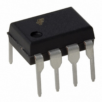
FSDM0365RNB Fairchild Semiconductor, FSDM0365RNB Datasheet - Page 13

FSDM0365RNB
Manufacturer Part Number
FSDM0365RNB
Description
IC SWIT PWM GREEN CM OVP HV 8DIP
Manufacturer
Fairchild Semiconductor
Datasheet
1.FSDM0365RNB.pdf
(20 pages)
Specifications of FSDM0365RNB
Output Isolation
Isolated
Frequency Range
61 ~ 73kHz
Voltage - Input
8 ~ 20 V
Voltage - Output
650V
Power (watts)
30W
Operating Temperature
25°C ~ 140°C
Package / Case
8-DIP (0.300", 7.62mm)
Lead Free Status / RoHS Status
Lead free / RoHS Compliant
Other names
FSDM0365RNB_NL
FSDM0365RNB_NL
FSDM0365RNB_NL
Available stocks
Company
Part Number
Manufacturer
Quantity
Price
Company:
Part Number:
FSDM0365RNB
Manufacturer:
Maxim
Quantity:
11
Company:
Part Number:
FSDM0365RNB
Manufacturer:
Fairchi/ON
Quantity:
15 000
Part Number:
FSDM0365RNB
Manufacturer:
FAIRCHILD/仙童
Quantity:
20 000
4.2 Thermal Shutdown (TSD) : The Sense FET and the
control IC are integrated, making it easier for the control IC
to detect the temperature of the Sense FET. When the tem-
perature exceeds approximately 140°C, thermal shutdown is
activated.
4.3 Over Voltage Protection (OVP) : In case of malfunc-
tion in the secondary side feedback circuit, or feedback loop
open caused by a defect of solder, the current through the
opto-coupler transistor becomes almost zero. Then, Vfb
climbs up in a similar manner to the over load situation, forc-
ing the preset maximum current to be supplied to the SMPS
until the over load protection is activated. Because excess
energy is provided to the output, the output voltage may
exceed the rated voltage before the over load protection is
activated, resulting in the breakdown of the devices in the
secondary side. In order to prevent this situation, an over
voltage protection (OVP) circuit is employed. In general,
Vcc is proportional to the output voltage and the FPS uses
Vcc instead of directly monitoring the output voltage. If
V
mination of the switching operation. In order to avoid undes-
ired activation of OVP during normal operation, Vcc should
be properly designed to be below 19V.
5. Soft Start : The FPS has an internal soft start circuit that
increases the feedback voltage together with the Sense FET
current slowly after it starts up. The typical soft start time is
15msec, as shown in figure 7, where progressive increments
of Sense FET current are allowed during the start-up phase.
The pulse width to the power switching device is progres-
sively increased to establish the correct working conditions
for transformers, inductors, and capacitors. The voltage on
the output capacitors is progressively increased with the
intention of smoothly establishing the required output volt-
Vcc
OLP
CC
8V
6V
3V
exceeds 19V, OVP circuit is activated resulting in ter-
t
1 t
t
2
1
=
=
C
FPS switching
−
fb
RC
(
1
V
fb
1 (
t
Delay current (5uA) charges the Cfb
Figure 6. Over load protection
In
2 t
+
I
1 (
t
delay
) 2
−
−
V
V
(
R
(
t
t
) 1
)) 1
);
;
V
I
delay
(
t
) 1
=
=
5
3
uA
V
,
,
3 t
V
R
1 (
t
=
+
2
8 .
t
) 2
K
−
Ω
V
,
C
(
t
Following Vcc
) 1
fb
=
=
3
4 t
C
V
fb
_
fig
2 .
t
age. It also helps to prevent transformer saturation and
reduce the stress on the secondary diode.
0.4A
6. Burst operation :In order to minimize power dissipation
in standby mode, the FPS enters burst mode operation.
As the load decreases, the feedback voltage decreases. As
shown in figure 9, the device automatically enters burst
mode when the feedback voltage drops below
V
limit is set to a fixed limit internally to minimize flux density
in the transformer. The fixed current limit is larger than that
defined by Vfb = V
further. Switching continues until the feedback voltage drops
below V
2.15A
0.98A
FB
BURH
3
Drain current
[A]
(500mV). Switching still continues but the current
BURL
I
delay
0.3/0.5V
S W I T C H
1mS
Vcc
0.5V
O F F
Figure 7. Soft Start Function
Figure 8. Circuit for Burst operation
(350mV). At this point switching stops and
Vcc
+
-
BURH
15steps
I
14steps
FB
5 V
2.5R
and therefore, Vfb is driven down
Current limit
I_ o v e r
R
FSDL0365RNB, FSDM0365RNB
Normal
R s e n s e
Burst
D R A I N
G N D
Vcc
I
B_PEAK
MOSFET
Current
PWM
13
t


