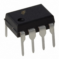
FSDL321 Fairchild Semiconductor, FSDL321 Datasheet

FSDL321
Specifications of FSDL321
FSDL321_NL
Related parts for FSDL321
FSDL321 Summary of contents
Page 1
... FSDH321, FSDL321 Green Mode Fairchild Power Switch (FPS Features • Internal Avalanche Rugged Sense FET • Consumes only 0.65W at 240VAC & 0.3W load with Advanced Burst-Mode Operation • Frequency Modulation for low EMI • Precision Fixed Operating Frequency • Internal Start-up Circuit • ...
Page 2
... FSDH321, FSDL321 Internal Block Diagram + V /V BURL BURH - V BURH Vcc Vcc I I delay 2. Vcc Vovp TSD 2 Vcc 2 Soft start 8V/12V Vcc good Vcc Freq. Modulation I B_PEAK OSC Normal PWM Burst Vcc good R Q Figure 2. Functional Block Diagram of FSDx321 Vstr Drain 5 6,7,8 ...
Page 3
... The Drain pin is designed to connect directly to the primary lead of the trans- former and is capable of switching a maximum of 650V. Minimizing the length of the trace connecting this pin to the transformer will decrease leak- age inductance. 8DIP 8LSOP Drain GND 1 8 Vcc 2 Drain 7 Vfb 6 Drain 3 Ipk 4 5 Vstr Figure 3. Pin Configuration (Top View) FSDH321, FSDL321 3 ...
Page 4
... FSDH321, FSDL321 Absolute Maximum Ratings (Ta=25°C, unless otherwise specified) Parameter Maximum Vstr Pin Voltage Maximum Drain Pin Voltage Drain-Gate Voltage (R =1MΩ) GS Gate-Source (GND) Voltage (1) Drain Current Pulsed Continuous Drain Current (Tc=25°C) Continuous Drain Current (Tc=100°C) Single Pulsed Avalanche Energy ...
Page 5
... DS C OSS f=1MHz C RSS td(on) V =0. DSS I =1. (MOSFET switching time td(off) is essentially independent of tf operating temperature) V =10V, I =1.0A =0. DSS (MOSFET switching time Qgs is essentially independent of operating Qgd temperature) FSDH321, FSDL321 Min. Typ. Max. Unit µ µ 200 Ω 1.0 1 162 - - 3 9 ...
Page 6
... FSDH321, FSDL321 Electrical Characteristics (Control Part) (Ta=25°C unless otherwise specified) Parameter UVLO SECTION Start Threshold Voltage Stop Threshold Voltage OSCILLATOR SECTION Initial Accuracy Frequency Modulation Initial Accuracy Frequency Modulation Frequency Change With Temperature Maximum Duty Cycle FEEDBACK SECTION Feedback Source Current ...
Page 7
... Programmable of default current limit ±1.5KHz @50KHz ±3.0KHz @100KHz Yes-built into controller 7.62mm FSDH321, FSDL321 FSDx321 Advantages • Gradually increasing current limit during soft-start further reduces peak current and voltage component stresses • Eliminates external components used for soft-start in most applications • ...
Page 8
... FSDH321, FSDL321 Typical Performance Characteristics (Control Part) (These characteristic graphs are normalized 1.20 1.00 0.80 0.60 0.40 0.20 0.00 - emp[ ℃ ] Operating Frequency (Fosc) 1.20 1.00 0.80 0.60 0.40 0.20 0.00 - emp[ ℃ ] Maximum duty cycle (Dmax) 1.20 1.00 0.80 0.60 ...
Page 9
... T emp[ ℃ ] Peak current limit (I LIM 1.20 1.00 0.80 0.60 0.40 0.20 0.00 - emp[ ℃ ] Startup Charging Current (Ich) 1.20 1.00 0.80 0.60 0.40 0.20 0.00 - emp[ ℃ ] Over Voltage Protection (Vovp) FSDH321, FSDL321 100 150 ) 100 150 100 150 9 ...
Page 10
... FSDH321, FSDL321 Functional Description 1. Startup : In previous generations of Fairchild Power TM Switches (FPS ) the Vstr pin had an external resistor to the DC input voltage line. In this generation the startup resistor is replaced by an internal high voltage current source and a switch that shuts off when 15mS goes by after the supply voltage, Vcc, gets above 12V ...
Page 11
... It also helps to prevent transformer saturation and reduce the stress on the secondary diode. Rsense 0.7A 0.4A exceeds 19V, OVP circuit is activated resulting in ter- TM has an internal soft start circuit Drain current [A] FSDH321, FSDL321 TM uses Tss 11 ...
Page 12
... As can be seen in Figure 11, the fre- I B_PEAK quency changes from 97KHz to 100KHz (from 48.5KHz to 51.5KHz for FSDL321)in 4mS for the FSDH321. Frequency PWM modulation allows the use of a cost effective inductor instead input mode choke to satisfy the requirements of Burst world wide EMI limits ...
Page 13
... XkΩ 2kΩ, Since X represents the resistance of the parallel network, A can be calculated using the following equation (X/2.8kΩ)) Ω PWM comparator SenseFET Rsense Sense Layout Considerations FSDH321, FSDL321 13 ...
Page 14
... FSDH321, FSDL321 Typical application circuit 1. PC Auxiliary Power Circuit (10W Output Power) 140~ 375 VDC INPUT R 101 680k Ω Vstr IC 101 FSDx321 Drain 3 Vfb Vcc ZD1 C104 GND 19V 22nF 1 10W PC Auxiliary Power, 150~375VDC Input Power supply: It shows an auxiliary power for PC. Efficiency at 10W, 150/ 375VDC is ≥ ...
Page 15
... tio tio tio tio tio tio tio tio Electric Specification and Core and Bobbin ire W ire φ × φ × φ × φ × φ × φ × φ × φ × φ × φ × – – Vcc FSDH321, FSDL321 15 ...
Page 16
... FSDH321, FSDL321 DC_link Capacitor #1 : GND #2 : VCC #3 : Vfb #4 : Ipk #5 : Vstr #6 : Drain #7 : Drain #8 : Drain Figure 13. Layout Considerations for FSDx321 using 8DIP 16 SURFACE MOUNTED COPPER AREA FOR HEAT SINKING - + DC OUT Y1- CAPACITOR ...
Page 17
... Package Dimensions 8DIP FSDH321, FSDL321 17 ...
Page 18
... FSDH321, FSDL321 Package Dimensions 18 (Continued) 8LSOP ...
Page 19
... Ordering Information Product Number Package FSDH321 8DIP FSDL321 8DIP FSDH321L 8LSOP FSDL321L 8LSOP Marking Code BV DSS DH321 650V DL321 650V DH321 650V DL321 650V FSDH321, FSDL321 F R OSC DS(on) 100KHz 14Ω 50KHz 14Ω 100KHz 14Ω 50KHz 14Ω 19 ...
Page 20
... FSDH321, FSDL321 DISCLAIMER FAIRCHILD SEMICONDUCTOR RESERVES THE RIGHT TO MAKE CHANGES WITHOUT FURTHER NOTICE TO ANY PRODUCTS HEREIN TO IMPROVE RELIABILITY, FUNCTION OR DESIGN. FAIRCHILD DOES NOT ASSUME ANY LIABILITY ARISING OUT OF THE APPLICATION OR USE OF ANY PRODUCT OR CIRCUIT DESCRIBED HEREIN; NEITHER DOES IT CONVEY ANY LICENSE UNDER ITS PATENT RIGHTS, NOR THE RIGHTS OF OTHERS. ...


