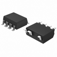
FSD200BM Fairchild Semiconductor, FSD200BM Datasheet - Page 10

FSD200BM
Manufacturer Part Number
FSD200BM
Description
IC SWIT PWM GREEN UVLO HV 7SOP
Manufacturer
Fairchild Semiconductor
Datasheet
1.FSD200BM.pdf
(18 pages)
Specifications of FSD200BM
Output Isolation
Isolated
Frequency Range
126 ~ 142kHz
Voltage - Input
6 ~ 10 V
Voltage - Output
670V
Power (watts)
7W
Operating Temperature
25°C ~ 100°C
Package / Case
8-SOP (7 Leads)
Power Switch Family
FSD200
Input Voltage
-0.3 to 10V
Power Switch On Resistance
28Ohm
Number Of Outputs
Single
Mounting
Surface Mount
Supply Current
600uA
Package Type
SOP
Operating Temperature (min)
-25C
Operating Temperature (max)
85C
Operating Temperature Classification
Commercial
Pin Count
7
Power Dissipation
1450W
Lead Free Status / RoHS Status
Lead free / RoHS Compliant
Other names
FSD200BM_NL
FSD200BM_NL
FSD200BM_NL
Available stocks
Company
Part Number
Manufacturer
Quantity
Price
Company:
Part Number:
FSD200BM/FSD200M
Manufacturer:
FAI
Quantity:
1 950
Company:
Part Number:
FSD200BMX
Manufacturer:
FSC
Quantity:
2 000
Company:
Part Number:
FSD200BMX
Manufacturer:
EUDYNA
Quantity:
100
FSD210B, FSD200B
4. Protection Circuit : The FSD200B/210B have 2 self-
protection functions : over load protection (OLP) and
thermal shutdown (TSD). Because these protection circuits
are fully integrated inside the IC without external compo-
nents, the reliability is improved without increasing cost.
Once a fault condition occurs, switching is terminated and
the Sense FET remains off. This causes Vcc to fall. When
Vcc reaches the UVLO stop voltage V
FSD210B, 6V-FSD200B), the protection is reset and the
internal high voltage current source charges the Vcc
capacitor via the Vstr pin. When Vcc reaches the UVLO
start voltage V
device resumes its normal operation. In this manner, the
auto-restart can alternately enable and disable the switching
of the power Sense FET until the fault condition is elimi-
nated.
4.1 Over Load Protection (OLP) : Overload is defined as
the load current exceeding a pre-set level due to an
unexpected event. In this situation, the protection circuit
should be activated in order to protect the SMPS. However,
even when the SMPS is operating normally, the over load
protection (OLP) circuit can be activated during the load
transition. In order to avoid this undesired operation, the
OLP circuit is designed to be activated after a specified time
to determine whether it is a transient situation or an overload
situation. In conjunction with the Ipk current limit pin (if
used) the current mode feedback path would limit the current
in the Sense FET when the maximum PWM duty cycle is
attained. If the output consumes more than this maximum
power, the output voltage (Vo) decreases below its rating
voltage. This reduces the current through the opto-coupler
LED, which also reduces the opto-coupler transistor current,
thus increasing the feedback voltage (V
3V, the feedback input diode is blocked and the 5uA current
source (I
this condition, V
switching operation is terminated as shown in Figure 10. The
shutdown delay time is the time required to charge Cfb from
3V to 4.5V with 5uA current source.
10
DELAY
Cfb
Vfb
4
START
Figure 9. Protection Block
) starts to charge Cfb slowly up to Vcc. In
FB
5uA
RESET
increases until it reaches 4.5V, when the
400uA
(8.7V-FSD210B, 7V-FSD200B), the
R
4.5V
OLP
+
-
TSD
OSC
A/R
S
R
S
R
FB
Q
Q
). If V
Protection Block
STOP
OLP, TSD
FSD2xxB
DRIVER
GATE
FB
exceeds
(6.7V-
4.2 Thermal Shutdown (TSD) : The Sense FET and the
control IC are integrated, making it easier for the control IC
to detect the temperature of the Sense FET. When the
temperature exceeds approximately 145°C, thermal
shutdown is activated.
5. Soft Start : FSD200B/210B has an internal soft start
circuit that gradually increases current through the Sense
FET as shown in Figure 11. The soft start time is 3msec in
FSD200B/210B.
4.5V
V
3V
t
I(A)
FB
12
=
C
Figure 10. Over Load Protection (OLP)
FB
0.2A
V
(
t
I
2
)
DELAY
Figure 11. Internal Soft Start
t
1
−
V
(
3ms
t
1
)
;
t
12
= C
I
DELAY
0.25A
Over Load Protection
FB
×
=
(V(t
5
µ
2
A
)-V(t
,
V
(
t
1
1
)) / I
)
=
0.3A
3
DELAY
V
,
V
(
t
2
)
=
t
2
4
5 .
V
t
t


