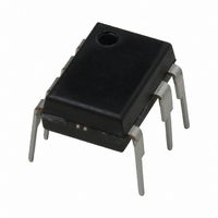
FSD200 Fairchild Semiconductor, FSD200 Datasheet

FSD200
Specifications of FSD200
FSD200_NL
Available stocks
Related parts for FSD200
FSD200 Summary of contents
Page 1
... Internal Thermal Shutdown Function (TSD) • Auto-Restart Mode • Frequency Modulation for EMI • FSD200 does not require an auxiliary bias winding Applications • Charger & Adaptor for Mobile Phone, PDA & MP3 • Auxiliary Power for White Goods, PC, C-TV & Monitor ...
Page 2
... Internal Block Diagram Vcc 5 UVLO Frequency Modulation 250uA 5uA Vfb 4 Reset Vcc 5 7V Frequency Modulation 5uA 250uA Vfb 4 Reset Figure 4. Functional Block Diagram of FSD200 showing internal high voltage regulator 2 Internal Voltage Bias Ref 8.7/6.7V Vck OSC BURST V BURST OLP TSD A/R Figure 3 ...
Page 3
... The startup pin connects directly to the rectified AC line voltage source for both the FSD200 and FSD210. For the FSD210, at start up the internal switch supplies internal bias and charges an external storage capacitor placed between the Vcc pin and ground. Once this reaches 8.7V, the internal current source is disabled ...
Page 4
... FSD210, FSD200 Absolute Maximum Ratings (Ta=25 C unless otherwise specified) Parameter Maximum Supply Voltage (FSD200) Maximum Supply Voltage (FSD210) Input Voltage Range Operating Junction Temperature. Operating Ambient Temperature Storage Temperature Range Thermal Impedance Parameter 7DIP Junction-to-Ambient Thermal Junction-to-Case Thermal 7LSOP Junction-to-Ambient Thermal ...
Page 5
... Feedback Shutdown Delay Current (2) Leading Edge Blanking Time TOTAL DEVICE SECTION Operating Supply Current (FSD200) Operating Supply Current (FSD210) Start Up Current (FSD200) Start Up Current (FSD210) Vstr Supply Voltage Note: 1. These parameters, although guaranteed, are not 100% tested in production 2. This parameter is derived from characterization ...
Page 6
... FSD210, FSD200 Comparison Between FSDH565 and FSD210 Function Soft-Start not applicable Switching Frequency 100kHz Frequency Modulation not applicable Burst Mode Operation not applicable Drain Creepage at 1.02mm Package 6 FSDH0565 FSD210 3mS 134kHz ±4kHz Yes-built into controller 3.56mm DIP 3.56mm LSOP FSD210 Advantages • ...
Page 7
... FSD210, FSD200 - 100 Junction Temperature (℃) Operating Current vs. Temp - 100 Junction Temperature (℃) Feedback Source Current vs. Temp - 100 Junction Temperature (℃) Vstop Voltage vs ...
Page 8
... Junction Temperature (℃) Breakdown Voltage vs. Temp - Junction Temperature (℃) Shutdown Feedback Voltage vs. Temp - Junction Temperature (℃) Start Up Current vs. Temp (for FSD200) 100 125 100 125 100 125 ...
Page 9
... Sense FET is turned on Protection Circuit : The FSD200/210 has 2 self protec- tion functions: over load protection (OLP) and thermal shut- down (TSD). Because these protection circuits are fully integrated into the IC with no external components, system ...
Page 10
... A/R Protection Block 5. Soft Start : FSD200/210 has an internal soft start circuit that gradually increases current through the Sense FET as shown in figure 11. The soft start time is 3msec in FSD200/ 210. I(A) 6. Burst operation : In order to minimize the power dissipa- tion in standby mode, the FSD200/210 implements burst mode functionality (see figure 12) ...
Page 11
... As can be seen in Figure 14, the frequency changes from 130kHz to 138kHz in 4mS for the FSD200/FSD210. Frequency modulation allows the use of a cost effective inductor instead input mode choke to satisfy the requirements of world wide EMI limits. ...
Page 12
... FSD210, FSD200 Typical application circuit Application Output power Cellular Phone Charger Features • High efficiency (>67% at Universal Input) • Low zero load power consumption (<100mW at 240Vac) with FSD210 • Low component count • Enhanced system reliability through various protection functions • Internal soft-start (3ms) • ...
Page 13
... FSD210, FSD200 Requirement/Comment Requirement/Comment DO41 Type DO41 Type DO41 Type DO41 Type D0-213 Type D0-213 Type D0-41 Type D0-41 Type TO-92 Type TO-92 Type Iover=0.3A, Fairchildsemi Iover=0.3A, Fairchildsemi ...
Page 14
... Ultra Fast Diode 1 Ic=200mA, Vcc=40V 12VZD/0. 0.5A/700V Output voltage (Max current) 12V (100mA) D2 UF4004 R2 110 D3(ZD) 1N759A C5 47uF 50V R3 VOUT(12V/100mA) 750 L1 1mH C4 R 1000uF 16V Requirement/Comment Requirement/Comment DO41 Type DO41 Type TO-92 Type DO-35 Type Iover=0.3A FSD210, FSD200 8.2K GND 14 ...
Page 15
... Layout Considerations (for Flyback Convertor GND #2 : GND #3 : GND #4 : Vfb #5 : Vcc # Drain #8 : Vstr Figure 17. Layout Considerations for FSD2x0 using 7DIP FSD210, FSD200 Copper area for heatsink 15 ...
Page 16
... FSD210, FSD200 Package Dimensions 16 7-DIP ...
Page 17
... Package Dimensions (Continued) 7-LSOP FSD210, FSD200 17 ...
Page 18
... FSD210, FSD200 Ordering Information Product Number FSD210 FSD200 FSD210M FSD200M DISCLAIMER FAIRCHILD SEMICONDUCTOR RESERVES THE RIGHT TO MAKE CHANGES WITHOUT FURTHER NOTICE TO ANY PRODUCTS HEREIN TO IMPROVE RELIABILITY, FUNCTION OR DESIGN. FAIRCHILD DOES NOT ASSUME ANY LIABILITY ARISING OUT OF THE APPLICATION OR USE OF ANY PRODUCT OR CIRCUIT DESCRIBED HEREIN; NEITHER DOES IT CONVEY ANY LICENSE UNDER ITS PATENT RIGHTS, NOR THE RIGHTS OF OTHERS ...


