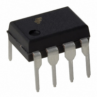
FSQ110 Fairchild Semiconductor, FSQ110 Datasheet - Page 3
FSQ110
Manufacturer Part Number
FSQ110
Description
IC SWIT PWM GREEN CM OVP 8DIP
Manufacturer
Fairchild Semiconductor
Datasheet
1.FSQ110.pdf
(12 pages)
Specifications of FSQ110
Output Isolation
Isolated
Frequency Range
92 ~ 108kHz
Voltage - Input
9 ~ 20 V
Voltage - Output
650V
Power (watts)
12W
Operating Temperature
25°C ~ 140°C
Package / Case
8-DIP (0.300", 7.62mm)
On Resistance (max)
14 Ohms
Maximum Operating Temperature
+ 85 C
Minimum Operating Temperature
- 25 C
Maximum Power Dissipation
1400 mW
Mounting Style
Through Hole
Supply Current
3 mA
Lead Free Status / RoHS Status
Lead free / RoHS Compliant
Available stocks
Company
Part Number
Manufacturer
Quantity
Price

Part Number:
FSQ110
Manufacturer:
FAIRCHILD/仙童
Quantity:
20 000
Part Number:
FSQ110 Q110
Manufacturer:
FAIRCHILD/仙童
Quantity:
20 000


FSQ110 Rev. 1.0.0
© 2007 Fairchild Semiconductor Corporation
Pin Configuration
Pin Definitions
Pin #
1
2
3
4
5
6
7
8
Name
GND
V
V
FB
I
PK
D
D
D
CC
str
Ground. SenseFET source terminal on primary side and internal control ground.
Power Supply. Positive supply voltage input. Although connected to an auxiliary trans-
former winding, current is supplied from pin 5 (V
(see Figure 2). It is not until V
nal start-up switch opens and device power is supplied via the auxiliary transformer wind-
ing.
Feedback. The feedback voltage pin is the non-inverting input to the PWM comparator.
It has a 0.9mA current source connected internally, while a capacitor and opto-coupler
are typically connected externally. A feedback voltage of 6V triggers overload protection
(OLP). A time delay while charging external capacitor C
5µA current source delay prevents false triggering under transient conditions, but still al-
lows the protection mechanism to operate under true overload conditions.
Peak Current Limit. This pin adjusts the peak current limit of the SenseFET. The 0.9mA
feedback current source is diverted to the parallel combination of an internal 2.8kΩ resis-
tor and any external resistor to GND on this pin. This determines the peak current limit.
If this pin is tied to V
Start-up. This pin connects to the rectified AC line voltage source. At start-up, the internal
switch supplies internal bias and charges an external storage capacitor placed between
the V
SenseFET Drain. High-voltage power SenseFET drain connection.
SenseFET Drain. High-voltage power SenseFET drain connection.
SenseFET Drain. High-voltage power SenseFET drain connection.
CC
pin and ground. Once the V
Figure 3. Pin Configuration (Top View)
GND
V
FB
I
CC
PK
CC
or left floating, the typical peak current limit is 0.7A.
FSQ110
8-DIP
CC
3
reaches the UVLO upper threshold (12V) that the inter-
CC
Description
reaches 12V, the internal switch is opened.
V
D
D
D
str
str
) via an internal switch during start-up
FB
from 3V to 6V using an internal
www.fairchildsemi.com
Related parts for FSQ110
Image
Part Number
Description
Manufacturer
Datasheet
Request
R

Part Number:
Description:
Fairchild Semiconductor [IGBT MODULE]
Manufacturer:
Fairchild Semiconductor
Datasheet:

Part Number:
Description:
Discrete Semiconductor Modules
Manufacturer:
Fairchild Semiconductor
Part Number:
Description:
Discrete Semiconductor Modules
Manufacturer:
Fairchild Semiconductor
Part Number:
Description:
This N-Channel MOSFET is produced using Fairchild Semiconductor’s advanced Power Trench® process
Manufacturer:
Fairchild Semiconductor
Datasheet:
Part Number:
Description:
This N-Channel MOSFET is produced using Fairchild Semiconductor’s advanced Power Trench® process
Manufacturer:
Fairchild Semiconductor
Datasheet:
Part Number:
Description:
This N-Channel MOSFET is produced using Fairchild Semiconductor’s advanced PowerTrench® process
Manufacturer:
Fairchild Semiconductor
Datasheet:
Part Number:
Description:
This N-Channel MOSFET is produced using Fairchild Semiconductor’s advanced PowerTrench® process
Manufacturer:
Fairchild Semiconductor
Datasheet:
Part Number:
Description:
This N-Channel MOSFET is produced using Fairchild Semiconductor’s advanced Power Trench® process
Manufacturer:
Fairchild Semiconductor
Datasheet:
Part Number:
Description:
This N-Channel logic Level MOSFETs are produced using Fairchild Semiconductor‘s advanced Power Trench® process that has been special tailored to minimize the on-state resistance and yet maintain superior switching performance
Manufacturer:
Fairchild Semiconductor
Datasheet:
Part Number:
Description:
This N-Channel MOSFET is produced using Fairchild Semiconductor’s advanced Power Trench® process
Manufacturer:
Fairchild Semiconductor
Datasheet:
Part Number:
Description:
This N-Channel SyncFET™ is produced using Fairchild Semiconductor’s advanced PowerTrench® process
Manufacturer:
Fairchild Semiconductor
Datasheet:
Part Number:
Description:
This N-Channel SyncFET™ is produced using Fairchild Semiconductor’s advanced PowerTrench® process
Manufacturer:
Fairchild Semiconductor
Datasheet:
Part Number:
Description:
This N-Channel SyncFET™ is produced using Fairchild Semiconductor’s advanced PowerTrench® process
Manufacturer:
Fairchild Semiconductor
Datasheet:
Part Number:
Description:
This N-Channel logic Level MOSFETs are produced using Fairchild Semiconductor‘s advanced Power Trench® process that has been special tailored to minimize the on-state resistance and yet maintain superior switching performance
Manufacturer:
Fairchild Semiconductor
Datasheet:
Part Number:
Description:
This N-Channel MOSFET is produced using Fairchild Semiconductor’s advanced Power Trench® process that has been especially tailored to minimize the on-state resistance and yet maintain superior switching performance
Manufacturer:
Fairchild Semiconductor
Datasheet: