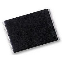
NAND256W3A2BN6E NUMONYX, NAND256W3A2BN6E Datasheet - Page 57

NAND256W3A2BN6E
Manufacturer Part Number
NAND256W3A2BN6E
Description
IC FLASH 256MBIT 48TSOP
Manufacturer
NUMONYX
Datasheet
1.NAND128W3A2BN6E.pdf
(59 pages)
Specifications of NAND256W3A2BN6E
Format - Memory
FLASH
Memory Type
FLASH - Nand
Memory Size
256M (32M x 8)
Interface
Parallel
Voltage - Supply
2.7 V ~ 3.6 V
Operating Temperature
-40°C ~ 85°C
Package / Case
48-TSOP
Access Time
12µs
Supply Voltage Range
1.7V To 1.95V, 2.7V To 3.6V
Memory Case Style
TSOP
No. Of Pins
48
Base Number
256
Block Size
16896Byte
Memory Configuration
32k X 8
Rohs Compliant
Yes
Lead Free Status / RoHS Status
Lead free / RoHS Compliant
Speed
-
Lead Free Status / RoHS Status
Lead free / RoHS Compliant, Lead free / RoHS Compliant
Other names
497-5038
497-5038
497-5038
Available stocks
Company
Part Number
Manufacturer
Quantity
Price
Company:
Part Number:
NAND256W3A2BN6E
Manufacturer:
ST
Quantity:
11 245
Company:
Part Number:
NAND256W3A2BN6E
Manufacturer:
MICRON/EOL43
Quantity:
444
Part Number:
NAND256W3A2BN6E
Manufacturer:
ST
Quantity:
20 000
NAND128-A, NAND256-A
13
Revision history
Table 24.
28-May-2004
07-Aug-2003
03-Dec-2003
03-Dec-2004
06-Jun-2003
27-Oct-2003
13-Apr-2004
01-Oct-2004
02-Jul-2004
Date
Document revision history
Version
1
2
3
4
5
6
7
8
9
Initial release
Design phase
Engineering phase
Document promoted from Target Specification to Preliminary Data status.
V
Changed title of
timing for NANDXXXR3A devices corrected.
NAND256-A device
WSOP48 and VFBGA55 packages added, VFBGA63 (9 x 11 x 1mm)
removed.
Figure 19: Cache Program
removed for t
address, data
t
characteristics for
References removed from
reference made to ST website instead.
Figure 5: VFBGA55 connections, x8 devices (top view through
Figure 6: VFBGA55 connections, x16 devices (top view through
package),
Figure 30: Block erase AC waveform
electronic signature
waveform, modified. Note 2 to
waveform
program operation. Note added to
Small text changes.
TFBGA55 package added (mechanical data to be announced). 512-Mbit
dual die devices added.
Package code changed for TFBGA63 8.5 x 15 x 1.2 mm, 6x8 ball array,
0.8 mm pitch (1-Gbit dual die devices) in
scheme.
Cache Program removed from document. TFBGA55 package
specifications added
array - 0.80mm pitch, Package Outline
10mm - 6x8 active ball array - 0.80mm pitch, Package Mechanical
Test conditions modified for V
Section 6.5: Block erase
block modified in
added to
Document promoted from Preliminary Data to Full Datasheet status.
Automatic Page 0 Read at power-up option no longer available.
PC Demo board with simulation software removed from list of available
development tools.
WHBH1
CC
changed to V
and t
Section 1:
removed. Only 00h pointer operations are valid before a cache
Figure 27: Page read A/read B operation AC waveform
WHRL
WLWH
input. Meaning of t
Table 2: Product description
Section 7.1: Bad block
DD
operations.
min for 3 V devices modified in
timing in
Section 3.5: Chip Enable (E)
clarified and
Description.
summary, inserted on page 2.
(Figure 40., TFBGA55 8 x 10mm - 6x8 active ball
and I
Figure 19., Cache Program Operation
last address cycle modified. Definition of a bad
CC
Section 13: Revision history
Operation, modified and note 2 modified. Note
Revision details
Table 19: AC characteristics for command,
OL
to I
Figure 28: Read C operation, one page AC
and V
Figure 2: Logic block diagram
DD
Figure 26: Read electronic signature AC
BLBH4
Figure 30: Block erase AC
.
modified.
OH
modified, partly replaced by
and
management. RoHS compliance
Table 23: Ordering information
parameters.
Table 25., TFBGA55 8 x
Table 1: NAND128-A and
and page program typical
Section 6.8: Read
paragraph clarified.
Table 20: AC
Revision history
section and
waveform.
package),
modified.
modified.
and
Data).
57/59


