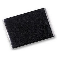
NAND256W3A2BN6E NUMONYX, NAND256W3A2BN6E Datasheet - Page 19

NAND256W3A2BN6E
Manufacturer Part Number
NAND256W3A2BN6E
Description
IC FLASH 256MBIT 48TSOP
Manufacturer
NUMONYX
Datasheet
1.NAND128W3A2BN6E.pdf
(59 pages)
Specifications of NAND256W3A2BN6E
Format - Memory
FLASH
Memory Type
FLASH - Nand
Memory Size
256M (32M x 8)
Interface
Parallel
Voltage - Supply
2.7 V ~ 3.6 V
Operating Temperature
-40°C ~ 85°C
Package / Case
48-TSOP
Access Time
12µs
Supply Voltage Range
1.7V To 1.95V, 2.7V To 3.6V
Memory Case Style
TSOP
No. Of Pins
48
Base Number
256
Block Size
16896Byte
Memory Configuration
32k X 8
Rohs Compliant
Yes
Lead Free Status / RoHS Status
Lead free / RoHS Compliant
Speed
-
Lead Free Status / RoHS Status
Lead free / RoHS Compliant, Lead free / RoHS Compliant
Other names
497-5038
497-5038
497-5038
Available stocks
Company
Part Number
Manufacturer
Quantity
Price
Company:
Part Number:
NAND256W3A2BN6E
Manufacturer:
ST
Quantity:
11 245
Company:
Part Number:
NAND256W3A2BN6E
Manufacturer:
MICRON/EOL43
Quantity:
444
Part Number:
NAND256W3A2BN6E
Manufacturer:
ST
Quantity:
20 000
NAND128-A, NAND256-A
4
4.1
4.2
4.3
Bus operations
There are six standard bus operations that control the memory. Each of these is described
in this section, see
Command input
Command input bus operations give commands to the memory. Commands are accepted
when Chip Enable is Low, Command Latch Enable is High, Address Latch Enable is Low,
and Read Enable is High. They are latched on the rising edge of the Write Enable signal.
Only I/O0 to I/O7 input commands.
See
program erase endurance cycles
Address input
Address input bus operations input the memory address. Three bus cycles are required to
input the addresses (refer to Tables
Address insertion, x16
The addresses are accepted when Chip Enable is Low, Address Latch Enable is High,
Command Latch Enable is Low, and Read Enable is High. They are latched on the rising
edge of the Write Enable signal. Only I/O0 to I/O7 input addresses.
See
program erase endurance cycles
Data input
Data input bus operations input the data to be programmed.
Data is accepted only when Chip Enable is Low, Address Latch Enable is Low, Command
Latch Enable is Low, and Read Enable is High. The data is latched on the rising edge of the
Write Enable signal and is input sequentially using the Write Enable signal.
See
program erase endurance cycles
of the timings requirements.
Figure 21: Command Latch AC waveforms
Figure 22: Address Latch AC waveforms
Figure 23: Data Input Latch AC waveforms
Table 5: Bus operations
devices).
for details of the timings requirements.
for details of the timings requirements.
and
Table 6: Address insertion, x8 devices
Table 20: AC characteristics for operations
for a summary.
and
and
and
Table 14: Program, erase times and
Table 14: Program, erase times and
Table 14: Program, erase times and
and
Bus operations
Table 7:
for details
19/59


