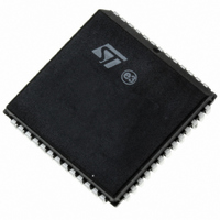
PSD813F1A-90JI STMicroelectronics, PSD813F1A-90JI Datasheet - Page 93

PSD813F1A-90JI
Manufacturer Part Number
PSD813F1A-90JI
Description
IC FLASH 1MBIT 90NS 52PLCC
Manufacturer
STMicroelectronics
Datasheet
1.PSD813F1A-90U.pdf
(111 pages)
Specifications of PSD813F1A-90JI
Format - Memory
FLASH
Memory Type
FLASH
Memory Size
1M (128K x 8)
Speed
90ns
Interface
Parallel
Voltage - Supply
4.5 V ~ 5.5 V
Operating Temperature
-40°C ~ 85°C
Package / Case
52-PLCC
Lead Free Status / RoHS Status
Contains lead / RoHS non-compliant
Other names
497-1976-5
Available stocks
Company
Part Number
Manufacturer
Quantity
Price
Company:
Part Number:
PSD813F1A-90JI
Manufacturer:
WSI
Quantity:
10
Company:
Part Number:
PSD813F1A-90JI
Manufacturer:
STMicroelectronics
Quantity:
10 000
Table 58. WRITE Timing (3V devices)
Note: 1. Any input used to select an internal PSD function.
Table 59. Flash Program, WRITE and Erase Times (5V devices)
Note: 1. Programmed to all zero before erase.
t
t
t
t
t
t
t
t
t
t
t
t
t
t
t
t
t
t
t
Symbol
LVLX
AVLX
LXAX
AVWL
SLWL
DVWH
WHDX
WLWH
WHAX1
WHAX2
WHPV
DVMV
AVPV
WLMV
WHQV3
WHQV2
WHQV1
WHWLO
Q7VQV
Symbol
2. In multiplexed mode, latched address generated from ADIO delay to address output on any port.
3. WR has the same timing as E, LDS, UDS, WRL, and WRH signals.
4. Assuming data is stable before active WRITE signal.
5. Assuming WRITE is active before data becomes valid.
6. TWHAX2 is the address hold time for DPLD inputs that are used to generate Sector Select signals for internal PSD memory.
2. The polling status, DQ7, is valid t
ALE or AS Pulse Width
Address Setup Time
Address Hold Time
Address Valid to Leading
Edge of WR
CS Valid to Leading Edge of WR
WR Data Setup Time
WR Data Hold Time
WR Pulse Width
Trailing Edge of WR to Address Invalid
Trailing Edge of WR to DPLD Address Invalid
Trailing Edge of WR to Port Output
Valid Using I/O Port Data Register
Data Valid to Port Output Valid
Using Macrocell Register Preset/Clear
Address Input Valid to Address
Output Delay
WR Valid to Port Output Valid Using
Macrocell Register Preset/Clear
Flash Program
Flash Bulk Erase
Flash Bulk Erase (not pre-programmed)
Sector Erase (pre-programmed)
Sector Erase (not pre-programmed)
Byte Program
Program / Erase Cycles (per Sector)
Sector Erase Time-Out
DQ7 Valid to Output (DQ7-DQ0) Valid (Data Polling)
Parameter
1
(pre-programmed)
Q7VQV
Parameter
time units before the data byte, DQ0-DQ7, is valid for reading.
Conditions
(Notes
(Notes
(Notes
(Note
(Note
(Note
(Note
(Note
(Note
(Note
(Note
(Note
(Note
2
3,6
1,3
3,5
3,4
1
1
3
3
3
3
3
3
2
)
)
)
)
)
)
)
)
)
)
)
)
)
100,000
Min.
Min
26
10
12
20
20
45
48
12
8
0
-15
Max
Typ.
100
45
90
48
90
8.5
2.2
10
14
3
1
Min
30
12
14
25
25
50
10
53
17
0
Max.
1200
30
30
30
-20
PSD813F1A
Max
100
100
50
55
cycles
Unit
93/111
µs
ns
µs
s
s
s
s
s
Unit
ns
ns
ns
ns
ns
ns
ns
ns
ns
ns
ns
ns
ns


