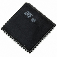
PSD834F2-90J STMicroelectronics, PSD834F2-90J Datasheet - Page 69

PSD834F2-90J
Manufacturer Part Number
PSD834F2-90J
Description
IC FLASH 2MBIT 90NS 52PLCC
Manufacturer
STMicroelectronics
Datasheet
1.PSD813F2VA-20JI.pdf
(109 pages)
Specifications of PSD834F2-90J
Format - Memory
FLASH
Memory Type
FLASH
Memory Size
2M (256K x 8)
Speed
90ns
Interface
Parallel
Voltage - Supply
4.5 V ~ 5.5 V
Operating Temperature
0°C ~ 70°C
Package / Case
52-PLCC
Lead Free Status / RoHS Status
Contains lead / RoHS non-compliant
Other names
497-2006-5
Available stocks
Company
Part Number
Manufacturer
Quantity
Price
Company:
Part Number:
PSD834F2-90J
Manufacturer:
STMicroelectronics
Quantity:
10 000
Part Number:
PSD834F2-90J
Manufacturer:
WSI
Quantity:
20 000
Company:
Part Number:
PSD834F2-90JI
Manufacturer:
SANYO
Quantity:
120
Company:
Part Number:
PSD834F2-90JI
Manufacturer:
STMicroelectronics
Quantity:
10 000
Part Number:
PSD834F2-90JI
Manufacturer:
WSI
Quantity:
20 000
PROGRAMMING IN-CIRCUIT USING THE JTAG SERIAL INTERFACE
The JTAG Serial Interface block can be enabled
on Port C (see
blocks (primary and secondary Flash memory),
PLD logic, and PSD Configuration Register bits
may be programmed through the JTAG Serial In-
terface block. A blank device can be mounted on
a printed circuit board and programmed using
JTAG.
The standard JTAG signals (IEEE 1149.1) are
TMS, TCK, TDI, and TDO. Two additional signals,
TSTAT and TERR, are optional JTAG extensions
used to speed up Program and Erase cycles.
By default, on a blank PSD (as shipped from the
factory or after erasure), four pins on Port C are
enabled for the basic JTAG signals TMS, TCK,
TDI, and TDO.
See Application Note AN1153 for more details on
JTAG In-System Programming (ISP).
Standard JTAG Signals
The standard JTAG signals (TMS, TCK, TDI, and
TDO) can be enabled by any of three different con-
ditions that are logically ORed. When enabled,
TDI, TDO, TCK, and TMS are inputs, waiting for a
JTAG serial command from an external JTAG con-
troller device (such as FlashLINK or Automated
Test Equipment). When the enabling command is
received, TDO becomes an output and the JTAG
channel is fully functional inside the PSD. The
same command that enables the JTAG channel
may optionally enable the two additional JTAG sig-
nals, TSTAT and TERR.
The following symbolic logic equation specifies the
conditions enabling the four basic JTAG signals
(TMS, TCK, TDI, and TDO) on their respective
Port C pins. For purposes of discussion, the logic
label JTAG_ON is used. When JTAG_ON is true,
the four pins are enabled for JTAG. When
JTAG_ON is false, the four pins can be used for
general PSD I/O.
JTAG_ON = PSDsoft_enabled +
/* An NVM configuration bit inside the
PSD is set by the designer in the
PSDsoft Express Configuration utility.
Table 34., page
70). All memory
Doc ID 10552 Rev 3
Microcontroller_enabled +
PSD_product_term_enabled;
The state of the PSD Reset (RESET) signal does
not interrupt (or prevent) JTAG operations if the
JTAG pins are dedicated by an NVM configuration
bit (via PSDsoft Express). However, Reset (RE-
SET) will prevent or interrupt JTAG operations if
the JTAG enable register is used to enable the
JTAG pins.
The PSD supports JTAG In-System-Configuration
(ISC) commands, but not Boundary Scan. The
PSDsoft Express software tool and FlashLINK
JTAG programming cable implement the JTAG In-
System-Configuration (ISC) commands. A defini-
tion of these JTAG In-System-Configuration (ISC)
commands and sequences is defined in a supple-
mental document available from ST. This docu-
ment is needed only as a reference for designers
who use a FlashLINK to program their PSD.
/* The microcontroller can set a bit at
/* A dedicated product term (PT) inside
This dedicates the pins for JTAG at all
times (compliant with IEEE 1149.1 */
run-time by writing to the PSD
register, JTAG Enable. This register is
located at address CSIOP + offset C7h.
Setting the JTAG_ENABLE bit in this
register will enable the pins for JTAG
use. This bit is cleared by a PSD reset
or the microcontroller. See
35., page 71
the PSD can be used to enable the JTAG
pins. This PT has the reserved name
JTAGSEL. Once defined as a node in
PSDabel, the designer can write an
equation for JTAGSEL. This method is
used when the Port C JTAG pins are
multiplexed with other I/O signals. It
is recommended to logically tie the
node JTAGSEL to the JEN\ signal on the
Flashlink cable when multiplexing JTAG
signals. See Application Note 1153 for
details. */
PSD813F2V, PSD854F2V
for bit definition. */
Table
69/109


