PSD834F2-90J STMicroelectronics, PSD834F2-90J Datasheet - Page 21
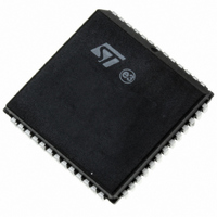
PSD834F2-90J
Manufacturer Part Number
PSD834F2-90J
Description
IC FLASH 2MBIT 90NS 52PLCC
Manufacturer
STMicroelectronics
Datasheet
1.PSD813F2VA-20JI.pdf
(109 pages)
Specifications of PSD834F2-90J
Format - Memory
FLASH
Memory Type
FLASH
Memory Size
2M (256K x 8)
Speed
90ns
Interface
Parallel
Voltage - Supply
4.5 V ~ 5.5 V
Operating Temperature
0°C ~ 70°C
Package / Case
52-PLCC
Lead Free Status / RoHS Status
Contains lead / RoHS non-compliant
Other names
497-2006-5
Available stocks
Company
Part Number
Manufacturer
Quantity
Price
Company:

Part Number:
PSD834F2-90J
Manufacturer:
STMicroelectronics
Quantity:
10 000
Part Number:
PSD834F2-90J
Manufacturer:
WSI
Quantity:
20 000
Company:
Part Number:
PSD834F2-90JI
Manufacturer:
SANYO
Quantity:
120
Company:
Part Number:
PSD834F2-90JI
Manufacturer:
STMicroelectronics
Quantity:
10 000
Part Number:
PSD834F2-90JI
Manufacturer:
WSI
Quantity:
20 000


Table 9. Instructions
Note: 1. All bus cycles are WRITE bus cycles, except the ones with the “READ” label
READ
Read Main
Flash ID
Read Sector
Protection
Program a
Flash Byte
Flash Sector
Erase
Flash Bulk
Erase
Suspend
Sector Erase
Resume
Sector Erase
Reset
Unlock Bypass
Unlock Bypass
Program
Unlock Bypass
Reset
Instruction
10. The Unlock Bypass Reset Flash instruction is required to return to reading memory data when the device is in the Unlock Bypass
11. The system may perform READ and Program cycles in non-erasing sectors, read the Flash ID or read the Sector Protection Status
12. The Resume Sector Erase instruction is valid only during the Suspend Sector Erase mode.
13. The MCU cannot invoke these instructions while executing code from the same Flash memory as that for which the instruction is
2. All values are in hexadecimal:
3. Sector Select (FS0 to FS7 or CSBOOT0 to CSBOOT3) signals are active High, and are defined in PSDsoft Express.
4. Only address bits A11-A0 are used in instruction decoding.
5. No Unlock or instruction cycles are required when the device is in the READ Mode
6. The Reset instruction is required to return to the READ Mode after reading the Flash ID, or after reading the Sector Protection Sta-
7. Additional sectors to be erased must be written at the end of the Sector Erase instruction within 80µs.
8. The data is 00h for an unprotected sector, and 01h for a protected sector. In the fourth cycle, the Sector Select is active, and
9. The Unlock Bypass instruction is required prior to the Unlock Bypass Program instruction.
7,13
13
6
10
5
X = Don’t Care. Addresses of the form XXXXh, in this table, must be even addresses
RA = Address of the memory location to be read
RD = Data read from location RA during the READ cycle
PA = Address of the memory location to be programmed. Addresses are latched on the falling edge of Write Strobe (WR, CNTL0).
PA is an even address for PSD in word programming mode.
PD = Data word to be programmed at location PA. Data is latched on the rising edge of Write Strobe (WR, CNTL0)
SA = Address of the sector to be erased or verified. The Sector Select (FS0-FS7 or CSBOOT0-CSBOOT3) of the sector to be
erased, or verified, must be Active (High).
tus, or if the Error Flag Bit (DQ5/DQ13) goes High.
(A1,A0)=(1,0)
mode.
when in the Suspend Sector Erase mode. The Suspend Sector Erase instruction is valid only during a Sector Erase cycle.
intended. The MCU must fetch, for example, the code from the secondary Flash memory when reading the Sector Protection Status
of the primary Flash memory.
6
9
6,8,13
13
11
12
FS0-FS7 or
CSBOOT0-
CSBOOT3
1
1
1
1
1
1
1
1
1
1
1
1
“READ”
RD @ RA
AAh@
X555h
AAh@
X555h
AAh@
X555h
AAh@
X555h
AAh@
X555h
B0h@
XXXXh
30h@
XXXXh
F0h@
XXXXh
AAh@
X555h
A0h@
XXXXh
90h@
XXXXh
Cycle 1
55h@
XAAAh
55h@
XAAAh
55h@
XAAAh
55h@
XAAAh
55h@
XAAAh
55h@
XAAAh
PD@ PA
00h@
XXXXh
Cycle 2
Doc ID 10552 Rev 3
90h@
X555h
90h@
X555h
A0h@
X555h
80h@
X555h
80h@
X555h
20h@
X555h
Cycle 3
Read identifier
(A6,A1,A0 = 0,0,1)
Read identifier
(A6,A1,A0 = 0,1,0)
PD@ PA
AAh@ X555h
AAh@ X555h
Cycle 4
PSD813F2V, PSD854F2V
55h@
XAAAh
55h@
XAAAh
Cycle 5
30h@
SA
10h@
X555h
Cycle 6
30h
next SA
Cycle 7
21/109
7
@
Related parts for PSD834F2-90J
Image
Part Number
Description
Manufacturer
Datasheet
Request
R

Part Number:
Description:
Flash In-System Programmable (ISP) Peripherals for 8-bit MCUs, 5V
Manufacturer:
STMicroelectronics
Datasheet:

Part Number:
Description:
IC FLASH 2MBIT 70NS 52QFP
Manufacturer:
STMicroelectronics
Datasheet:
Part Number:
Description:
IC FLASH 2MBIT 90NS 52QFP
Manufacturer:
STMicroelectronics
Datasheet:

Part Number:
Description:
IC FLASH 2MBIT 70NS 52PLCC
Manufacturer:
STMicroelectronics
Datasheet:
Part Number:
Description:
IC FLASH 2MBIT 90NS 52PLCC
Manufacturer:
STMicroelectronics
Datasheet:
Part Number:
Description:
IC FLASH 2MBIT 90NS 52QFP
Manufacturer:
STMicroelectronics
Datasheet:
Part Number:
Description:
Manufacturer:
STMicroelectronics
Datasheet:
Part Number:
Description:
Manufacturer:
STMicroelectronics
Datasheet:

Part Number:
Description:
Three Phase Rectifier Bridge
Manufacturer:
POWERSEM [Powersem GmbH]
Datasheet:
Part Number:
Description:
STMicroelectronics [RIPPLE-CARRY BINARY COUNTER/DIVIDERS]
Manufacturer:
STMicroelectronics
Datasheet:
Part Number:
Description:
STMicroelectronics [LIQUID-CRYSTAL DISPLAY DRIVERS]
Manufacturer:
STMicroelectronics
Datasheet:

Part Number:
Description:
BOARD EVAL FOR MEMS SENSORS
Manufacturer:
STMicroelectronics
Datasheet: