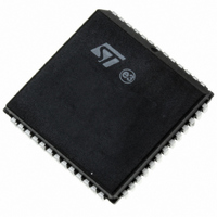
PSD834F2-90J STMicroelectronics, PSD834F2-90J Datasheet - Page 66

PSD834F2-90J
Manufacturer Part Number
PSD834F2-90J
Description
IC FLASH 2MBIT 90NS 52PLCC
Manufacturer
STMicroelectronics
Datasheet
1.PSD813F2VA-20JI.pdf
(109 pages)
Specifications of PSD834F2-90J
Format - Memory
FLASH
Memory Type
FLASH
Memory Size
2M (256K x 8)
Speed
90ns
Interface
Parallel
Voltage - Supply
4.5 V ~ 5.5 V
Operating Temperature
0°C ~ 70°C
Package / Case
52-PLCC
Lead Free Status / RoHS Status
Contains lead / RoHS non-compliant
Other names
497-2006-5
Available stocks
Company
Part Number
Manufacturer
Quantity
Price
Company:
Part Number:
PSD834F2-90J
Manufacturer:
STMicroelectronics
Quantity:
10 000
Part Number:
PSD834F2-90J
Manufacturer:
WSI
Quantity:
20 000
Company:
Part Number:
PSD834F2-90JI
Manufacturer:
SANYO
Quantity:
120
Company:
Part Number:
PSD834F2-90JI
Manufacturer:
STMicroelectronics
Quantity:
10 000
Part Number:
PSD834F2-90JI
Manufacturer:
WSI
Quantity:
20 000
PSD813F2V, PSD854F2V
PSD Chip Select Input (CSI, PD2)
PD2 of Port D can be configured in PSDsoft Ex-
press as PSD Chip Select Input (CSI). When Low,
the signal selects and enables the internal Flash
memory, EEPROM, SRAM, and I/O blocks for
READ or WRITE operations involving the PSD. A
High on PSD Chip Select Input (CSI, PD2) dis-
ables the Flash memory, EEPROM, and SRAM,
and reduces the PSD power consumption. How-
ever, the PLD and I/O signals remain operational
when PSD Chip Select Input (CSI, PD2) is High.
There may be a timing penalty when using PSD
Chip Select Input (CSI, PD2) depending on the
speed grade of the PSD that you are using. See
the timing parameter t
or
Table 32. APD Counter Operation
66/109
APD Enable Bit
Table 62., page
0
1
1
1
ALE PD Polarity
95.
SLQV
X
X
1
0
in
Table 61., page 94
ALE Level
Pulsing
Doc ID 10552 Rev 3
X
1
0
Not Counting
Counting (Generates PDN after 15 Clocks)
Counting (Generates PDN after 15 Clocks)
Not Counting
Input Clock
The PSD provides the option to turn off CLKIN
(PD1) to the PLD to save AC power consumption.
CLKIN (PD1) is an input to the PLD AND Array and
the Output Macrocells (OMC).
During Power-down mode, or, if CLKIN (PD1) is
not being used as part of the PLD logic equation,
the clock should be disabled to save AC power.
CLKIN (PD1) is disconnected from the PLD AND
Array or the Macrocells block by setting Bits 4 or 5
to a 1 in PMMR0.
Input Control Signals
The PSD provides the option to turn off the input
control signals (CNTL0, CNTL1, CNTL2, Address
Strobe (ALE/AS, PD0) and DBE) to the PLD to
save AC power consumption. These control sig-
nals are inputs to the PLD AND Array. During
Power-down mode, or, if any of them are not being
used as part of the PLD logic equation, these con-
trol signals should be disabled to save AC power.
They are disconnected from the PLD AND Array
by setting Bits 2, 3, 4, 5, and 6 to a 1 in PMMR2.
APD Counter


