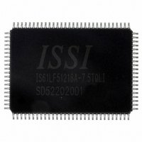
IS61LF51218A-7.5TQLI ISSI, Integrated Silicon Solution Inc, IS61LF51218A-7.5TQLI Datasheet - Page 19

IS61LF51218A-7.5TQLI
Manufacturer Part Number
IS61LF51218A-7.5TQLI
Description
IC SRAM 9MBIT 7.5NS 100TQFP
Manufacturer
ISSI, Integrated Silicon Solution Inc
Datasheet
1.IS61LF25636A-7.5TQLI-TR.pdf
(32 pages)
Specifications of IS61LF51218A-7.5TQLI
Format - Memory
RAM
Memory Type
SRAM - Synchronous
Memory Size
9M (512K x 18)
Speed
7.5ns
Interface
Parallel
Voltage - Supply
3.135 V ~ 3.6 V
Operating Temperature
-40°C ~ 85°C
Package / Case
100-TQFP, 100-VQFP
Lead Free Status / RoHS Status
Lead free / RoHS Compliant
Other names
706-1094
IS61LF51218A-7.5TQLI
IS61LF51218A-7.5TQLI
Available stocks
Company
Part Number
Manufacturer
Quantity
Price
Company:
Part Number:
IS61LF51218A-7.5TQLI
Manufacturer:
ISSI, Integrated Silicon Solution Inc
Quantity:
10 000
Company:
Part Number:
IS61LF51218A-7.5TQLI-TR
Manufacturer:
ISSI, Integrated Silicon Solution Inc
Quantity:
10 000
IS61/64LF25636A IS61LF51218A IS61VF25636A IS61VF51218A
IEEE 1149.1 SERIAL BOUNDARY SCAN (JTAG)
The IS61LF/VF25636A and IS61LF/VF51218A have a
serial boundary scan Test Access Port (TAP) in the PBGA
package only. This port operates in accordance with IEEE
Standard 1149.1-1900, but does not include all functions
required for full 1149.1 compliance. These functions from
the IEEE specification are excluded because they place
added delay in the critical speed path of the SRAM. The
TAP controller operates in a manner that does not conflict
with the performance of other devices using 1149.1 fully
compliant TAPs. The TAP operates using JEDEC standard
2.5V I/O logic levels.
DISABLING THE JTAG FEATURE
The SRAM can operate without using the JTAG feature.
To disable the TAP controller, TCK must be tied LOW
(Vss) to prevent clocking of the device. TDI and TMS are
internally pulled up and may be disconnected. They may
alternately be connected to V
TDO should be left disconnected. On power-up, the device
will start in a reset state which will not interfere with the
device operation.
TAP CONTROLLER BLOCK DIAGRAM
Integrated Silicon Solution, Inc.
Rev. H
07/22/2010
TMS
TCK
TDI
Selection Circuitry
TAP CONTROLLER
dd
through a pull-up resistor.
31 30 29
0
2
x
Bypass Register
Instruction Register
Identification Register
Boundary Scan Register*
. . . . .
1
0
. . .
TEST ACCESS PORT (TAP) - TEST CLOCK
The test clock is only used with the T AP controller. All inputs
TEST MODE SELECT (TMS)
The TMS input is used to send commands to the TAP
is internally pulled up, resulting in a logic HIGH level.
TEST DATA-IN (TDI)
The TDI pin is used to serially input information to the
registers and can be connected to the input of any regis-
can be disconnected if the TAP is unused in an applica-
are captured on the rising edge of TCK and outputs are
driven from the falling edge of TCK.
controller and is sampled on the rising edge of TCK. This
pin may be left disconnected if the TAP is not used. The pin
ter. The register between TDI and TDO is chosen by the
instruction loaded into the TAP instruction register. For
information on instruction register loading, see the TAP
Controller State Diagram. TDI is internally pulled up and
tion. TDI is connected to the Most Significant Bit (MSB)
on any register.
2
2
1
1
0
0
Selection Circuitry
TDO
19


