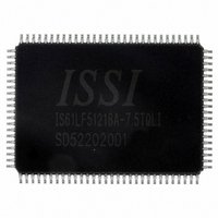
IS61LF51218A-7.5TQLI ISSI, Integrated Silicon Solution Inc, IS61LF51218A-7.5TQLI Datasheet - Page 10

IS61LF51218A-7.5TQLI
Manufacturer Part Number
IS61LF51218A-7.5TQLI
Description
IC SRAM 9MBIT 7.5NS 100TQFP
Manufacturer
ISSI, Integrated Silicon Solution Inc
Datasheet
1.IS61LF25636A-7.5TQLI-TR.pdf
(32 pages)
Specifications of IS61LF51218A-7.5TQLI
Format - Memory
RAM
Memory Type
SRAM - Synchronous
Memory Size
9M (512K x 18)
Speed
7.5ns
Interface
Parallel
Voltage - Supply
3.135 V ~ 3.6 V
Operating Temperature
-40°C ~ 85°C
Package / Case
100-TQFP, 100-VQFP
Lead Free Status / RoHS Status
Lead free / RoHS Compliant
Other names
706-1094
IS61LF51218A-7.5TQLI
IS61LF51218A-7.5TQLI
Available stocks
Company
Part Number
Manufacturer
Quantity
Price
Company:
Part Number:
IS61LF51218A-7.5TQLI
Manufacturer:
ISSI, Integrated Silicon Solution Inc
Quantity:
10 000
Company:
Part Number:
IS61LF51218A-7.5TQLI-TR
Manufacturer:
ISSI, Integrated Silicon Solution Inc
Quantity:
10 000
IS61/64LF25636A IS61LF51218A IS61VF25636A IS61VF51218A
TRUTH TABLE
NOTE:
10
1. X means “Don’t Care.” H means logic HIGH. L means logic LOW.
2. For WRITE, L means one or more byte write enable signals (BWa-d) and BWE are LOW or GW is LOW. WRITE = H for all
3. BWa enables WRITEs to DQa’s and DQPa. BWb enables WRITEs to DQb’s and DQPb. BWc enables WRITEs to DQc’s and
4. All inputs except OE and ZZ must meet setup and hold times around the rising edge (LOW to HIGH) of CLK.
5. Wait states are inserted by suspending burst.
6. For a WRITE operation following a READ operation, OE must be HIGH before the input data setup time and held HIGH during
7. This device contains circuitry that will ensure the outputs will be in High-Z during power-up.
8. ADSP LOW always initiates an internal READ at the L-H edge of CLK. A WRITE is performed by setting one or more byte write
OPERATION
Deselect Cycle, Power-Down
Deselect Cycle, Power-Down
Deselect Cycle, Power-Down
Deselect Cycle, Power-Down
Deselect Cycle, Power-Down
Snooze Mode, Power-Down
Read Cycle, Begin Burst
Read Cycle, Begin Burst
Write Cycle, Begin Burst
Read Cycle, Begin Burst
Read Cycle, Begin Burst
Read Cycle, Continue Burst
Read Cycle, Continue Burst
Read Cycle, Continue Burst
Read Cycle, Continue Burst
Write Cycle, Continue Burst
Write Cycle, Continue Burst
Read Cycle, Suspend Burst
Read Cycle, Suspend Burst
Read Cycle, Suspend Burst
Read Cycle, Suspend Burst
Write Cycle, Suspend Burst
Write Cycle, Suspend Burst
PARTIAL TRUTH TABLE
Function
Read
Read
Write Byte 1
Write All Bytes
Write All Bytes
BWx, BWE, GW HIGH.
DQPc. BWd enables WRITEs to DQd’s and DQPd. DQPa and DQPb are available on the x18 version. DQPa-DQPd are avail-
able on the x36 version.
the input data hold time.
enable signals and BWE LOW or GW LOW for the subsequent L-H edge of CLK. See WRITE timing diagram for clarification.
(1-8)
GW
H
H
H
H
L
ADDRESS CE
External
External
External
External
External
Current
Current
Current
Current
Current
Current
None
None
None
None
None
None
Next
Next
Next
Next
Next
Next
BWE
H
X
L
L
L
H
X
X
X
H
H
X
H
X
X
H
H
X
H
L
L
L
L
L
L
L
L
L
BWa
H
X
L
L
X
CE2 CE2
H
H
X
X
X
X
L
L
L
L
L
X
X
X
X
X
X
X
X
X
X
X
X
BWb
H
H
X
X
L
X
X
X
X
H
H
H
H
H
X
X
X
X
X
X
X
X
X
X
X
X
L
L
ZZ ADSP ADSC ADV WRITE OE CLK
BWc
H
L
L
L
L
L
L
L
L
L
L
L
L
L
L
L
L
L
L
L
L
L
L
H
H
X
X
L
X
H
H
X
H
H
H
H
H
X
X
H
X
H
H
X
X
H
X
L
L
L
L
BWd
X
H
H
X
L
X
X
X
X
X
H
H
H
H
H
H
H
H
H
H
H
H
L
L
L
L
L
L
H
H
H
H
H
H
X
X
X
X
X
X
X
X
X
X
X
L
L
L
L
L
L
Integrated Silicon Solution, Inc.
H
H
H
H
H
H
H
H
H
H
X
X
X
X
X
X
X
X
L
L
L
L
L
X
X
X
X
X
X
H
X
H
H
H
X
X
H
H
X
X
L
L
L
L
L
L
L-H
L-H
L-H
L-H
L-H
L-H
L-H
L-H
L-H
L-H
L-H
L-H
L-H
L-H
L-H
L-H
L-H
L-H
L-H
L-H
L-H
L-H
X
07/22/2010
High-Z
High-Z
High-Z
High-Z
High-Z
High-Z
High-Z
High-Z
High-Z
High-Z
High-Z
High-Z
DQ
Q
D
Q
Q
D
D
Q
Q
D
D
Rev. H
Q


