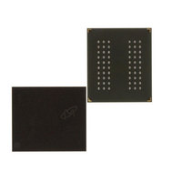
MT46H64M16LFCK-6 IT:A TR Micron Technology Inc, MT46H64M16LFCK-6 IT:A TR Datasheet - Page 35

MT46H64M16LFCK-6 IT:A TR
Manufacturer Part Number
MT46H64M16LFCK-6 IT:A TR
Description
IC DDR SDRAM 1GBIT 60VFBGA
Manufacturer
Micron Technology Inc
Type
DDR SDRAMr
Specifications of MT46H64M16LFCK-6 IT:A TR
Format - Memory
RAM
Memory Type
Mobile DDR SDRAM
Memory Size
1G (64M x 16)
Speed
166MHz
Interface
Parallel
Voltage - Supply
1.7 V ~ 1.95 V
Operating Temperature
-40°C ~ 85°C
Package / Case
60-VFBGA
Organization
64Mx16
Density
1Gb
Address Bus
14b
Access Time (max)
6.5/5.5ns
Maximum Clock Rate
166MHz
Operating Supply Voltage (typ)
1.8V
Package Type
VFBGA
Operating Temp Range
-40C to 85C
Operating Supply Voltage (max)
1.95V
Operating Supply Voltage (min)
1.7V
Supply Current
115mA
Pin Count
60
Mounting
Surface Mount
Operating Temperature Classification
Industrial
Lead Free Status / RoHS Status
Lead free / RoHS Compliant
Other names
557-1335-2
Figure 10: READ Command
WRITE
PDF: 09005aef82ce3074
1gb_ddr_mobile_sdram_t48m.pdf - Rev. K 07/09 EN
Note:
Address
The WRITE command is used to initiate a burst write access to an active row. The val-
ues on the BA0 and BA1 inputs select the bank; the address provided on inputs A[I:0]
(where I = the most significant column address bit for each configuration) selects the
starting column location. The value on input A10 determines whether auto precharge is
used. If auto precharge is selected, the row being accessed will be precharged at the end
of the WRITE burst; if auto precharge is not selected, the row will remain open for subse-
quent accesses. Input data appearing on the DQ is written to the memory array, subject
to the DM input logic level appearing coincident with the data. If a given DM signal is
registered LOW, the corresponding data will be written to memory; if the DM signal is
registered HIGH, the corresponding data inputs will be ignored, and a WRITE will not
be executed to that byte/column location.
If a WRITE or a READ is in progress, the entire data burst must be complete prior to
stopping the clock (see Clock Change Frequency (page 92)). A burst completion for
WRITEs is defined when the write postamble and
BA0,1
1. EN AP = enable auto precharge; DIS AP = disable auto precharge.
CAS#
RAS#
WE#
A10
CKE
CK#
CS#
CK
HIGH
Column
DIS AP
EN AP
Bank
Don’t Care
35
1Gb: x16, x32 Mobile LPDDR SDRAM
Micron Technology, Inc. reserves the right to change products or specifications without notice.
t
WR or
t
WTR are satisfied.
©2007 Micron Technology, Inc. All rights reserved.
Commands


