CLC031VEC National Semiconductor, CLC031VEC Datasheet - Page 7
CLC031VEC
Manufacturer Part Number
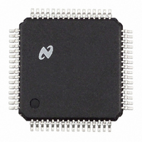
CLC031VEC
Description
IC DESERIAL/DESCRMBLR VID 64TQFP
Manufacturer
National Semiconductor
Type
Descrambler/Deserializerr
Datasheet
1.CLC031VEC.pdf
(31 pages)
Specifications of CLC031VEC
Applications
SDTV/HDTV
Mounting Type
Surface Mount
Package / Case
64-TQFP, 64-VQFP
Lead Free Status / RoHS Status
Contains lead / RoHS non-compliant
Other names
*CLC031VEC
Available stocks
Company
Part Number
Manufacturer
Quantity
Price


Serial Video Data Inputs
BR
t
Parallel Video Data Outputs
f
t
t
Parallel Ancilliary / Control Data Inputs, Multi-function Parallel Bus Inputs
f
DC
t
t
t
Parallel Ancilliary / Control Data Outputs
t
t
Multi-function Parallel I/O Bus
t
PLL/CDR, Format Detect
t
t
r
VCLK
pd
JIT
ACLK
r
S
H
pd
pd
r
LOCK
FORMAT
Symbol
, t
, t
, t
AC Electrical Characteristics
Over Supply Voltage and Operating Temperature ranges, unless otherwise specified (Note 3).
Note 1: “Absolute Maximum Ratings” are those parameter values beyond which the life and operation of the device cannot be guaranteed. The stating herein of
these maximums shall not be construed to imply that the device can or should be operated at or beyond these values. The table of “Electrical Characteristics”
specifies acceptable device operating conditions.
Note 2: Current flow into device pins is defined as positive. Current flow out of device pins is defined as negative. All voltages are referenced to V
V
SDI
f
A
f
f
SSSI
= 0V.
Serial Input Data Rate
Rise Time, Fall Time
Video Output Clock
Frequency
Propagation Delay, Video
Clock to Video Data Valid
Video Data Output Clock
Jitter
Ancilliary / Control Data
Clock Frequency
Ancilliary / Control Clock
Duty Cycle
Output Rise Time, Fall
Time
Setup Time, AD
or IO
Hold Time, Rising Edge
A
IO
Propagation Delay, Clock
to Control Data
Propagation Delay, Clock
to Ancilliary Data
Rise Time, Fall Time
Lock Detect Time
Format Detect Time
CLK
N
N
to AD
to A
Parameter
CLK
N
or A
Rising Edge
N
CLK
to A
to
CLK
SMPTE 259M, Level C
SMPTE 259M, Level D
SMPTE 344M
SMPTE 292M
SMPTE 292M
20%–80%, SMPTE 259M
Data Rates
20%–80%, SMPTE 292M
Data Rates
SMPTE 259M, 270M
SMPTE 267M, 360M
SMPTE 344M, 540M
SMPTE 292M, 1,483M
SMPTE 292M, 1,485M
50%–50%
27MHz
36MHz
54MHz
74.25MHz
ANC Data clock
(Note 7)
10%–90%
Control Data Input or I/O
Bus Input
50%–50%
10%–90%
SD Rates (Note 5)
HD Rates (Note 5)
All Rates
Conditions
BPS
BPS
BPS
BPS
BPS
7
SDI, SDI
V
V
Timing Diagram
V
A
IO
Timing Diagram
A
Timing Diagram
IO0–IO7
Timing Diagram
CLK
CLK
CLK
CLK
CLK
N
Reference
, AD
to DV
to AD
N
, A
N
N
CLK
Min
720
1.0
3.0
3.0
1.0
45
74.176
1,483
1,485
74.25
27.0
36.0
54.0
11.5
0.32
0.26
Typ
270
360
540
800
0.5
3.0
2.2
1.5
1.0
1.5
1.5
1.5
8.5
1.5
50
20
74.25
Max
880
270
2.0
3.0
3.0
1.0
1.0
55
SSIO
www.national.com
= V
Units
M
ns
MHz
MHz
SSD
ms
ps
ns
ns
ns
ns
%
BPS
P-P
=
Related parts for CLC031VEC
Image
Part Number
Description
Manufacturer
Datasheet
Request
R

Part Number:
Description:
Smpte 292m/259m Digital Video Deserializer / Descrambler With Video And Ancilliary Data Fifos
Manufacturer:
National Semiconductor Corporation
Datasheet:

Part Number:
Description:
National Semiconductor [8-Bit D/A Converter]
Manufacturer:
National Semiconductor
Datasheet:
Part Number:
Description:
National Semiconductor [Media Coprocessor]
Manufacturer:
National Semiconductor
Datasheet:
Part Number:
Description:
Digitally Controlled Tone and Volume Circuit with Stereo Audio Power Amplifier, Microphone Preamp Stage and National 3D Sound
Manufacturer:
National Semiconductor
Datasheet:
Part Number:
Description:
Digitally Controlled Tone and Volume Circuit with Stereo Audio Power Amplifier, Microphone Preamp Stage and National 3D Sound
Manufacturer:
National Semiconductor
Datasheet:
Part Number:
Description:
AC97 Rev 2 Codec with Sample Rate Conversion and National 3D Sound
Manufacturer:
National Semiconductor
Part Number:
Description:
Manufacturer:
National Semiconductor
Datasheet:
Part Number:
Description:
Manufacturer:
National Semiconductor
Datasheet:
Part Number:
Description:
General Purpose, Low Voltage, Low Power, Rail-to-Rail Output Operational Amplifiers
Manufacturer:
National Semiconductor
Datasheet:
Part Number:
Description:
8-bit 20 MSPS flash A/D converter.
Manufacturer:
National Semiconductor
Datasheet:
Part Number:
Description:
Low Noise Quad Operational Amplifier
Manufacturer:
National Semiconductor
Datasheet:
Part Number:
Description:
Quad Differential Line Receivers
Manufacturer:
National Semiconductor
Datasheet:
Part Number:
Description:
Quad High Speed Trapezoidal? Bus Transceiver
Manufacturer:
National Semiconductor
Datasheet:
Part Number:
Description:
Dual Line Receiver
Manufacturer:
National Semiconductor
Datasheet: