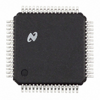
CLC031VEC National Semiconductor, CLC031VEC Datasheet - Page 11

CLC031VEC
Manufacturer Part Number
CLC031VEC
Description
IC DESERIAL/DESCRMBLR VID 64TQFP
Manufacturer
National Semiconductor
Type
Descrambler/Deserializerr
Datasheet
1.CLC031VEC.pdf
(31 pages)
Specifications of CLC031VEC
Applications
SDTV/HDTV
Mounting Type
Surface Mount
Package / Case
64-TQFP, 64-VQFP
Lead Free Status / RoHS Status
Contains lead / RoHS non-compliant
Other names
*CLC031VEC
Available stocks
Company
Part Number
Manufacturer
Quantity
Price
Device Operation
The SMPTE descrambler receives NRZI serial data, con-
verts it to NRZ, then decodes it to either 10-bit standard
definition or 20-bit high definition parallel video data using
the reverse polynomial X
respective standard: SMPTE 259M, SMPTE 344M (pro-
posed) or SMPTE 292M. The data reception bit order is
LSB-first. All data processing is done at the parallel rate.
The CLC031 incorporates circuitry that implements a
method for handling data that has been subjected to LSB
dithering. When so enabled, data from the de-scrambler is
routed for de-dithering. The De-Dither Enable bit in the
VIDEO INFO 0 control register enables this function. De-
dithering of data present in the vertical blanking interval can
be selectively enabled by use of the V De-Dither Enable bit
in the VIDEO INFO 0 control register. The initial condition of
De-Dither Enable and V De-Dither Enable is OFF.
The descrambler supplies signals to theTRS character de-
tector which identifies the presence of the valid video data.
The TRS character detector processes the timing refer-
ence signals which control raster framing. TRS (sync) char-
acters are detected and the video is aligned on word bound-
aries. Data is re-synchronized with the parallel word-rate
FIGURE 1. Optional Input Biasing Scheme
9
+ X
(Continued)
4
+ 1 as specified in the
20020106
11
clock. Interraction and operation of the character alignment
control signals and indicators Framing Mode, Framing En-
able and NSP (New Sync Position) is described later in this
datasheet.
The CLC031 implements TRS character LSB-clipping as
prescribed in ITU-R BT.601. LSB-clipping causes all TRS
characters with a value between 000h and 003h to be forced
to 000h and all TRS characters with a value between 3FCh
and 3FFh to be forced to 3FFh. Clipping is done after de-
scrambling and de-dithering.
Once the PLL attains lock, the video format detector pro-
cesses the received data to determine the raster character-
istics (video data format) and configure the CLC031 to
handle it. This assures that the parallel output data will be
properly formatted, that the correct data rate is selected and
that ancilliary data and CRC/EDH data are correctly de-
tected and checked. Supported parallel data formats or sub-
formats may belong to any one of several component stan-
dards: SMPTE 125M, SMPTE 267M, SMPTE 260M, 274M,
295M or 296M. Refer to Table 4 for the supported formats.
(See also the Application Information section for handling of
other raster formats or format extensions developed after
this device was designed). The detected video standard
information is passed to the device control system and
saved in the control registers from whence it may be read by
the user.
The CLC031 may be configured to operate in a single video
format by loading the appropriate FORMAT SET[4:0] control
data into the FORMAT 0 control register. Also, the CLC031
may be configured to handle only the standard-definition
data formats by setting the SD ONLY bit or only the high-
definition data formats by setting the HD ONLY bit in the
FORMAT 0 control register. When both bits are reset, the
default condition, the part automatically detects the data rate
and range.
Aligned and de-processed parallel data passes into a
variable-depth video FIFO prior to output. Video FIFO depth
from 0 to 4 registers is set by a 3-bit word written into the
VIDEO FIFO Depth[2:0] bits in the ANC 0 control register.
The video FIFO permits adjustment of the parallel video data
output timing or delay at a parallel word rate. The occurence
of corresponding TRS indicator bits, EAV, SAV and NSP, in
the control register corresponds to the input register position
of the FIFO. This positioning permits a look-ahead function
in which the alignment status of the video data can be
determined up to four parallel clock periods prior to the
appearance of that data at the parallel data output.
The parallel video data is output on DV[19:0]. The 20-bit
parallel video data is organized so that for HDTV data, the
upper-order 10 bits DV[19:10] are luminance (luma) infor-
mation and the lower 10 bits DV[9:0] are colour difference
(chroma) information. SDTV data use the lower-order 10-bits
DV[9:0] for both luma and chroma information. (The SDTV
parallel data is also duplicated on DV[19:10]). V
parallel output word rate clock signal. The frequency of V
is appropriate to either the HD or SD data being processed.
Data is valid between the falling edges of a V
may be clocked into external devices on the rising-edge of
V
compatible.
CLK
. The DV[19:0] and V
CLK
signals are LVCMOS-
CLK
www.national.com
cycle. Data
CLK
is the
CLK


