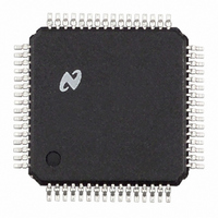
CLC031VEC National Semiconductor, CLC031VEC Datasheet - Page 14

CLC031VEC
Manufacturer Part Number
CLC031VEC
Description
IC DESERIAL/DESCRMBLR VID 64TQFP
Manufacturer
National Semiconductor
Type
Descrambler/Deserializerr
Datasheet
1.CLC031VEC.pdf
(31 pages)
Specifications of CLC031VEC
Applications
SDTV/HDTV
Mounting Type
Surface Mount
Package / Case
64-TQFP, 64-VQFP
Lead Free Status / RoHS Status
Contains lead / RoHS non-compliant
Other names
*CLC031VEC
Available stocks
Company
Part Number
Manufacturer
Quantity
Price
www.national.com
Device Operation
Figure 4 shows the relationship of clock, data and control
signals for reading Ancilliary Data from the port AD[9:0]. In
ancilliary data read mode, 10-bit ancilliary data is routed
from the Ancilliary Data FIFO and read from the port
AD[9:0] at a rate determined by A
Ancilliary data read (output) mode is invoked by making the
ANC/CTRL input high and the RD/WR input high. Ancilliary
Data is clocked from the FIFO on the L-H transition of A
Data may be read from the port on rising edges of A
after the specified propagation delay, until the FIFO is emp-
MULTI-FUNCTION I/O PORT
The multi-function I/O port can be configured to provide
immediate access to many control and indicator functions
that are stored within the CLC031’s configuration and control
registers. The individual pins comprising this port are as-
signed as input or output for selected functions stored in the
control data registers.
The multi-function I/O port is configured by way of an 8x6-bit
register bank consisting of registers I/O pin 0 CONFIG
through I/O pin 7 CONFIG. The contents of these registers
determine whether the port bits function as inputs or outputs
and to which control function or indicator each port bit is
assigned. Port bits may be assigned to access different
functions and indicators or any or all port bits may be as-
signed to access the same function or indicator (output
mode only). The same indicator or function should not be
assigned to more than one port bit as an input. Controls and
indicators that are accessible by the port and their corre-
sponding selection addresses are given in the I/O Pin Con-
figuration Register Addresses, Table 6. Table 2 gives the
control register bit assignments.
Data resulting from device operation will be sent to the
selected I/O port bit. This same data is also stored in the
configuration and control registers. Mapping the control and
indicator functions in this manner means that device opera-
tion will be immediately reflected at the I/O port pins thereby
ensuring more reliable real-time operation of the device
within and by the host system.
When a multifunction I/O port bit is used as input to a control
register bit, data must be presented to the I/O port bit and
clocked into the register bit using A
Port timing for bit write operations is the same as for the
ANC/CTRL port operation.
(Continued)
CLK
CLK
.
as shown in Figure 5.
FIGURE 4. Ancilliary Data Read Timing
CLK
CLK
.
,
14
tied. Data may only be read from the port when in the
ancilliary data mode. Ancilliary data cannot be written to the
port.
To conserve power when the ancilliary data function is not
being used, the internal Ancilliary Data FIFO clock is dis-
abled. This clock must be enabled before ancilliary data may
be replicated into the FIFO for output. This internal FIFO
clock is controlled by FIFO CLOCK ENABLE, bit-6 of the
ANC 5 register (address 17h). The default condition of FIFO
CLOCK ENABLE is OFF. After enabling the internal FIFO
clock by turning this bit ON, A
times to propagate the enable to the clock tree.
Example: Program multi-function I/O port bit-0 as the CRC
Luma Error bit output.
1. Set ANC/CTRL to a logic-low.
2. Set RD/WR to a logic-low.
3. Present 00Fh to AD[9:0] as the I/O PIN 0 CONFIG
4. Toggle A
5. Present 310h to AD[9:0] as the register data.
6. Toggle A
EDH/CRC SYSTEM
The CLC031 has EDH and CRC character generation and
checking circuitry. The EDH system functions as described
in SMPTE Recommended Practice RP-165. The CRC sys-
tem functions as specified in SMPTE 292M. The EDH/CRC
polynomial generators/checkers accept parallel data from
the de-serializing system and generate the EDH and CRC
check words for comparison with those received in the data.
The EDH Enable bit in the control register enables the EDH
generation and checking system. Incoming SDTV data is
checked for errors and the EDH flags are updated automati-
register address.
FIGURE 5. I/O Port Data Write Timing
CLK
CLK
.
.
CLK
20020111
must be toggled three (3)
20020112


