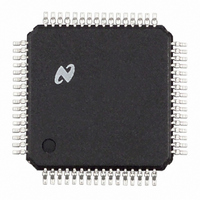
CLC031VEC National Semiconductor, CLC031VEC Datasheet - Page 10

CLC031VEC
Manufacturer Part Number
CLC031VEC
Description
IC DESERIAL/DESCRMBLR VID 64TQFP
Manufacturer
National Semiconductor
Type
Descrambler/Deserializerr
Datasheet
1.CLC031VEC.pdf
(31 pages)
Specifications of CLC031VEC
Applications
SDTV/HDTV
Mounting Type
Surface Mount
Package / Case
64-TQFP, 64-VQFP
Lead Free Status / RoHS Status
Contains lead / RoHS non-compliant
Other names
*CLC031VEC
Available stocks
Company
Part Number
Manufacturer
Quantity
Price
www.national.com
Timing Diagram
Device Operation
Introduction
The CLC031 SMPTE 292M/259M Digital Video Deserializer/
Decoder is used in digital video signal origination and desti-
nation equipment: cameras, video tape recorders, telecines,
editors, standards converters, video test and other equip-
ment. It decodes and converts serial SDTV or HDTV com-
ponent digital video signals into parallel format. The CLC031
decoder/deserializer processes serial digital video (SDV)
signals conforming to SMPTE 259M, SMPTE 344M (pro-
posed) or SMPTE 292M and operates at serial data rates of
270 Mbps, 360 Mbps, 540 Mbps, 1.483 Gbps and
1.485 Gbps. Corresponding parallel output data rates are
27.0 MHz, 36.0 MHz, 54.0 MHz, 74.176MHz and 74.25 MHz.
The CLC031 accepts ECL or LVDS serial data input signals.
Outputs signals are compatible with LVCMOS logic devices.
Note: In the following explanations, these logical equiva-
lences are observed: ON
and OFF
≡
Disabled
≡
Reset
≡
Enabled
≡
False
≡
Set
≡
Logic_0.
≡
True
≡
Logic_1
10
VIDEO DATA PATH
The Serial Data Inputs (SDI) accept serial video data at
SMPTE 259M standard definition, SMPTE 344M (proposed)
or SMPTE 292M high-definition data rates. These inputs
accept standard ECL or LVDS signal levels and may be used
single-ended or differentially. Inputs may be DC or AC
coupled, as required, to devices and circuits supplying the
data. Recommended operating conditions and all input DC
and AC voltage and current specifications shall be observed
when designing the input coupling circuits.
For convenience, a reference bias source, pin name R
sets the reference current available from the input bias
source, pin name R
R
may be supplied DC bias voltage via external resistors when
the inputs are AC-coupled. The bias source should be
loaded with a resistance to the V
current available at R
input biasing scheme using R
REF
is 4.75kΩ, 1%. R
BB
BB
. The recommended nominal value of
BB
is 200µA. Figure 1 shows a typical
is provided so that the SDI inputs
20020108
BB
and R
SS
REF
supply. The source
.
REF
,


