CLC031VEC National Semiconductor, CLC031VEC Datasheet
CLC031VEC
Specifications of CLC031VEC
Available stocks


Related parts for CLC031VEC


CLC031VEC Summary of contents
Page 1
... Ancilliary Data FIFO and Integrated Cable Driver, is the ideal complement to the CLC031. Ordering Information Order Number CLC031VEC © 2003 National Semiconductor Corporation The CLC031’s internal circuitry is powered from +2.5 Volts and the I/O circuitry from a +3.3 Volt supply. Power dissipa- tion is typically 850mW ...
Page 2
Typical Application www.national.com 2 20020101 ...
Page 3
Block Diagram 3 20020102 www.national.com ...
Page 4
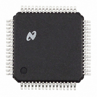
... Connection Diagram www.national.com 64-Pin TQFP Order Number CLC031VEC See NS Package Number VEC-64A 4 20020103 ...
Page 5
Absolute Maximum Ratings It is anticipated that this device will not be offered in a military qualified version. If Military/Aerospace speci- fied devices are required, please contact the National Semiconductor Sales Office / Distributors for availability and specifications. CMOS I/O ...
Page 6
Required Input Conditions Symbol Parameter Ancilliary / Control Data f ACLK Clock Frequency Ancilliary / Control Clock DC ACLK Duty Cycle Ancilliary / Control Clock and Data Rise Time, Fall r f Time Setup Time ...
Page 7
AC Electrical Characteristics Over Supply Voltage and Operating Temperature ranges, unless otherwise specified (Note 3). Symbol Parameter Serial Video Data Inputs BR Serial Input Data Rate SDI Rise Time, Fall Time r f Parallel Video Data Outputs ...
Page 8
AC Electrical Characteristics Note 3: Typical values are stated for DDIO Note 4: Spec. is guaranteed by design. Note 5: Measured from rising-edge of first SDI cycle until Lock Detect bit goes high (true). Lock time includes ...
Page 9
Test Circuit 9 20020107 www.national.com ...
Page 10
Timing Diagram Device Operation Introduction The CLC031 SMPTE 292M/259M Digital Video Deserializer/ Decoder is used in digital video signal origination and desti- nation equipment: cameras, video tape recorders, telecines, editors, standards converters, video test and other equip- ment. It decodes ...
Page 11
Device Operation (Continued) FIGURE 1. Optional Input Biasing Scheme The SMPTE descrambler receives NRZI serial data, con- verts it to NRZ, then decodes it to either 10-bit standard definition or 20-bit high definition parallel video data using 9 4 the ...
Page 12
Device Operation (Continued) ANCILLIARY/CONTROL DATA PATH The 10-bit Ancilliary and Control Data Port AD[9:0] serves two functions in the CLC031. Ancilliary data from the Ancilliary Data FIFO is output from this port after its recov- ery from the video data ...
Page 13
Device Operation (Continued) FIGURE 2. Control Data Read Timing (2 read and 1 write cycle shown) Ancilliary Data Functions The CLC031 can recover Ancilliary Data from the serial data stream. This ancilliary data and related control charac- ters are defined ...
Page 14
Device Operation (Continued) Figure 4 shows the relationship of clock, data and control signals for reading Ancilliary Data from the port AD[9:0]. In ancilliary data read mode, 10-bit ancilliary data is routed from the Ancilliary Data FIFO and read from ...
Page 15
Device Operation (Continued) cally. EDH errors are reported in the EDH0, EDH1, and EDH2 register sets of the configuration and control registers. Updated or new EDH check words and flags may be gener- ated and inserted in the data. EDH ...
Page 16
Device Operation (Continued) TEST PATTERN GENERATOR (TPG) AND BUILT-IN SELF-TEST (BIST) The CLC031 includes an on-board, parallel video test pat- tern generator (TPG). Four test pattern types are available in both HD and SD formats, NTSC and PAL standards, and ...
Page 17
Device Operation (Continued) TABLE 1. Configuration and Control Data Register Summary Register Function Bits EDH and CRC Operations CRC Error (SD/HD) 1 CRC Error Luma 1 CRC Error Chroma 1 CRC Replace 1 Full-Field Flags 5 Active Picture Flags 5 ...
Page 18
Device Operation (Continued) TABLE 1. Configuration and Control Data Register Summary (Continued) Register Function Bits Sync Detect Enable 1 De-Dither Enable 1 Vert. De-Dither Enable 1 Lock Detect 1 Unscrambled 1 Video Data Out TPG and BIST Operations Test Pattern ...
Page 19
Device Operation (Continued) TABLE 2. Control Register Bit Assignments (Continued) Bit 7 Bit 6 ANC FIFO SHORT MSG ANC PARITY 90% FULL DETECT FORMAT 0 (register address 0Bh) FRAMING SD ONLY HD ONLY MODE FORMAT 1 (register address 0Ch) F ...
Page 20
Device Operation (Continued) TABLE 3. Control Register Addresses Register Name EDH 0 EDH 1 EDH 2 ANC 0 ANC 1 ANC 2 ANC 3 ANC 4 ANC 5 ANC 6 FORMAT 0 FORMAT 1 TEST 0 VIDEO INFO 0 I/O ...
Page 21
Device Operation (Continued) reported via the ANC Checksum Error bit. ANC Checksum Error is available as an output on the multifunction I/O port. ANC 1 AND 2 (Addresses 05h and 06h) The extraction of ancilliary data packets from video data ...
Page 22
Device Operation (Continued) Format Code Format [4,3,2,1,0] 00001 SDTV 174 00010 SDTV, 36 SMPTE 267 00011 SDTV, 27 SMPTE 125 01001 SDTV, 54 ITU-R BT 601.5 01010 SDTV, 36 ITU-R BT 601.5 01011 SDTV, 27 ITU-R BT 601.5 ...
Page 23
Device Operation (Continued) > Test Pattern Select Word Bits Video Raster Standard 1125 Line, 74.25 MHz, 30 Frame Interlaced Component (SMPTE 260M) Ref. Black PLL Path. EQ Path. Colour Bars 1125 Line, 74.25 MHz, 30 Frame Interlaced Component (SMPTE 274M) ...
Page 24
Device Operation (Continued) > Test Pattern Select Word Bits 525 Line, 30 Frame, 27 MHz, NTSC 4x3 (SMPTE 125M) Ref. Black PLL Path. EQ Path. Colour Bars (SD BIST) 625 Line, 25 Frame, 27 MHz, PAL 4x3 (ITU-T BT.601) Ref. ...
Page 25
Device Operation (Continued) VIDEO CONTROL 0 (register address 55h) The EXTERNAL V bit is a special application function CLK which enables use of an external VCXO as a substitute for the internally generated V . Additional circuitry is enabled CLK ...
Page 26
Device Operation (Continued) TABLE 6. Control Register Bit, Pin[n] SEL[5:0] Codes for I/O Port Pin Mapping Register Bit [5] reserved 0 FF Flag Error 0 AP Flag Error 0 ANC Flag Error 0 CRC Error (SD/HD) 0 ANC FIFO 90% ...
Page 27
Pin Descriptions Pin Name 1 AD9 2 AD8 3 AD7 4 AD6 5 AD5 6 V SSD 7 AD4 8 AD3 9 AD2 10 AD1 11 AD0 12 V DDD 13 A CLK 14 IO7 15 IO6 16 IO5 17 ...
Page 28
Pin Descriptions (Continued) Pin Name 50 V CLK 51 V DDPLL 52 V SSPLL 53 R REF SSSI 56 SDI 57 SDI 58 V DDSI 59 V SSIO 60 XTALi/EXT CLK 61 XTALo 62 V ...
Page 29
Application Information The power pins feeding the I/O should have low inductance connections to the power and ground planes recom- mended that these connections use at least two vias per power or ground pin. Short interconnecting traces consistent ...
Page 30
Application Information The control voltage output from R BB the loop filter consisting of a 22.1kΩ resistor in series with a 10nF capacitor, combined in parallel with a 100pF capacitor. This gives a loop bandwidth of 1.5kHz. Since the control ...
Page 31
... National does not assume any responsibility for use of any circuitry described, no circuit patent licenses are implied and National reserves the right at any time without notice to change said circuitry and specifications. inches (millimeters) 64-Pin TQPF Order Number CLC031VEC NS Package Number VEC-64A 2. A critical component is any component of a life ...