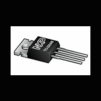
PSMN1R1-30PL NXP Semiconductors, PSMN1R1-30PL Datasheet - Page 7

PSMN1R1-30PL
Manufacturer Part Number
PSMN1R1-30PL
Description
Manufacturer
NXP Semiconductors
Datasheet
1.PSMN1R1-30PL.pdf
(15 pages)
NXP Semiconductors
Table 6.
[1]
PSMN1R1-30PL
Product data sheet
Symbol
t
t
t
t
Source-drain diode
V
t
Q
d(on)
r
d(off)
f
rr
Fig 5.
SD
r
Measured 3 mm from package.
(S)
g
300
240
180
120
fs
60
0
drain current; typical values
Forward transconductance as a function of
0
Characteristics
Parameter
turn-on delay time
rise time
turn-off delay time
fall time
source-drain voltage
reverse recovery time
recovered charge
20
…continued
40
60
All information provided in this document is subject to legal disclaimers.
003aaf762
I
D
(A)
Conditions
V
R
I
see
I
V
S
S
DS
GS
G(ext)
80
= 25 A; V
= 25 A; dI
Rev. 02 — 19 April 2011
Figure 17
= 15 V; R
= 0 V; V
= 5 Ω; I
GS
S
DS
N-channel 30 V 1.3 mΩ logic level MOSFET in TO-220
/dt = -100 A/µs;
L
D
= 0 V; T
Fig 6.
= 0.2 Ω; V
= 15 V
= 75 A; T
(A)
I
D
75
60
45
30
15
j
0
= 25 °C;
function of gate-source voltage; typical values
Transfer characteristics: drain current as a
0
j
GS
= 25 °C
= 4.5 V;
0.6
T
j
PSMN1R1-30PL
= 175 ° C
1.2
Min
-
-
-
-
-
-
-
1.8
Typ
95
213
199
115
0.8
67
123
© NXP B.V. 2011. All rights reserved.
T
2.4
j
003aaf763
= 25 ° C
V
GS
-
Max
-
-
-
1.2
-
-
(V)
3
Unit
ns
ns
ns
ns
V
ns
nC
7 of 15


