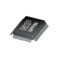
P8XC557E4 NXP Semiconductors, P8XC557E4 Datasheet - Page 47

P8XC557E4
Manufacturer Part Number
P8XC557E4
Description
The P80C557E4/P83C557E4/P89C557E4 (hereafter generically referred to as P8xC557E4) single-chip 8-bit microcontroller is manufactured in an advanced CMOS process and is a derivative of the 80C51 microcontroller family
Manufacturer
NXP Semiconductors
Datasheet
1.P8XC557E4.pdf
(72 pages)
Philips Semiconductors
7. INSTRUCTION SET
The P8xC557E4 uses the powerful instruction set of the PCB80C51.
It consists of 49 single-byte, 45 two-byte and 17 three-byte
instructions. Using a 16 MHz quartz, 64 of the instructions are
executed in 0.75 s, 45 in 1,5 s and the multiply, divide instructions
in 3 s.
A summary of the instruction set is given in Table 43.
The P8xC557E4 has additional Special Function Registers to
control the on-chip peripherals.
7.1 Addressing Modes
Most instructions have a “destination, source” field that specifies the
data type, addressing modes and operands involved. For all these
instructions, except for MOVs, the destination operand is also the
source operand (e.g., ADD A,R7).
There are five kinds of addressing modes:
The first three addressing modes are usable for destination
operands.
1999 Mar 02
Register Addressing
– R0 – R7 (4 banks)
– A,B,C (bit), AB (2 bytes), DPTR (double byte)
Direct Addressing
– lower 128 bytes of internal Main RAM (including the 4 R0–R7
– Special Function Registers
– 128 bits in a subset of the internal Main RAM
– 128 bits in a subset of the Special Function Registers
– internal Main RAM (@R0, @R1, @SP [PUSH/POP])
– internal Auxiliary RAM (@R0, @R1, @DPTR)
– external Data Memory (@R0, @R1, @DPTR)
– Program Memory (in-code 8 bit or 16 bit constant)
– Program Memory look-up table (@DPTR+A, @PC+A)
Single-chip 8-bit microcontroller
Register-Indirect Addressing
Immediate Addressing
Base-Register-plus Index-Register-Indirect Addressing
register banks)
47
P83C557E4/P80C557E4/P89C557E4
1. Note that operations on SFR byte address 208 or bit addresses
7.1.1 80C51 Family Instruction Set
Table 42. Instruction that affect Flag settings
NOTES:
Notes on instruction set and addressing modes:
Rn
direct
@Ri
#data
#data 16
addr 16
addr 11
rel
bit
Hexadecimal opcode cross-reference to Table 43:
209-215 (i.e., the PSW or bits in the PSW) will also affect flag
settings.
INSTRUCTION
ADD
ADDC
SUBB
MUL
DIV
DA
RRC
RLC
SETB C
CLR C
CPL C
ANL C, bit
ANL C,/bit
ANL C, bit
ORL C, bit
MOV C, bit
CJNE
*
**
***
:
:
:
Register R7-R0 of the currently selected Register
Bank.
8-bit internal data location’s address. This could be
an Internal Data RAM location (0-127) or a SFR
[i.e., I/O port, control register, status register, etc.
(128-255)].
8-bit RAM location addressed indirectly through
register R1 or R0 of the actual register bank.
8-bit constant included in the instruction.
16-bit constant included in the instruction
16-bit destination address. Used by LCALL and
LJMP. A branch can be anywhere within the
64 Kbytes Program Memory address space.
11-bit destination address. Used by ACALL and
AJMP. The branch will be within the same 2 Kbytes
page of program memory as the first byte of the
following instruction.
Signed (two’s complement) 8-bit offset byte. Used
by SJMP and all conditional jumps. Range is –128
to +127 bytes relative to first byte of the following
instruction.
Direct Addressed bit in Internal Data RAM or
Special Function Register.
8, 9, A, B, C, D, E. F.
11, 31, 51, 71, 91, B1, D1, F1.
01, 21, 41, 61, 81, A1, C1, E1.
C
X
X
X
X
X
X
X
X
X
X
X
X
X
0
0
1
0
FLAG
OV
X
X
X
X
X
X
Product specification
AC
X
X
X
1


