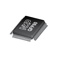
P8XC557E4 NXP Semiconductors, P8XC557E4 Datasheet - Page 18

P8XC557E4
Manufacturer Part Number
P8XC557E4
Description
The P80C557E4/P83C557E4/P89C557E4 (hereafter generically referred to as P8xC557E4) single-chip 8-bit microcontroller is manufactured in an advanced CMOS process and is a derivative of the 80C51 microcontroller family
Manufacturer
NXP Semiconductors
Datasheet
1.P8XC557E4.pdf
(72 pages)
- Current page: 18 of 72
- Download datasheet (375Kb)
Philips Semiconductors
Table 10. Description of ADCON bits
1999 Mar 02
SYMBOL
ADCON.7
ADCON.6
ADCON.5
ADCON.4
ADCON.3
ADCON.2
ADCON.1
ADCON.0
Single-chip 8-bit microcontroller
ADPR1
ADPR0
ADPOS
ADINT
ADSST
ADCSA
ADSRE
ADSFE
BIT
AV
AV
AV
AV
ADEXS
ADC0
ADC7
ref+
SS1
ref–
DD1
FUNCTION
Control bit for the prescaler.
Control bit for the prescaler.
ADPR1=0 ADPR0=0 Prescaler divides by 2 (default by reset)
ADPR1=0 ADPR0=1 Prescaler divides by 4
ADPR1=1 ADPR0=0 Prescaler divides by 6
ADPR1=1 ADPR0=1 Prescaler divides by 8
ADPOS is reserved for future use. Must be ’0’ if ADCON is written.
ADC interrupt flag. This flag is set when all selected analog inputs are converted, as well in continuous
scan as in one-time scan mode. An interrupt is invoked if this interrupt is enabled. ADINT must be cleared
by software. It cannot be set by software.
ADC start and status. Setting this bit by software or by hardware (via ADEXS input) starts the A/D
conversion of the selected analog inputs. ADSST stays a ‘one’ in continuous scan mode. In one-time scan
mode, ADSST is cleared by hardware when the last selected analog input channel has been converted. As
long as ADSST is ’1’, new start commands to the ADC-block are ignored.
An A/D conversion in progress is aborted if ADSST is cleared by software.
1
0
1
0
1
0
ADPSS
=
=
=
=
=
=
Continuous scan of the selected analog inputs after a start of an A/D conversion.
One-time scan of the selected analog inputs after a start of an A/D conversion.
A rising edge at input ADEXS will start the A/D conversion and generate a capture signal.
A rising edge at input ADEXS has no effect.
A falling edge at input ADEXS will start the A/D conversion and generate a capture signal.
A falling edge at input ADEXS has no effect.
8
SCAN LOGIC
Figure 15. Functional diagram of AD converter.
ANALOG
ADCON
Mux.
8
INTERNAL BUS
18
P83C557E4/P80C557E4/P89C557E4
COMPARATOR
DAC
ADRSH
Read
+
–
10–bit result
2 LATCHES
registers
8x
2
2
10
ADRSL
Read
SAR
10
10
n
8
8
Product specification
Related parts for P8XC557E4
Image
Part Number
Description
Manufacturer
Datasheet
Request
R
Part Number:
Description:
NXP Semiconductors designed the LPC2420/2460 microcontroller around a 16-bit/32-bitARM7TDMI-S CPU core with real-time debug interfaces that include both JTAG andembedded trace
Manufacturer:
NXP Semiconductors
Datasheet:

Part Number:
Description:
NXP Semiconductors designed the LPC2458 microcontroller around a 16-bit/32-bitARM7TDMI-S CPU core with real-time debug interfaces that include both JTAG andembedded trace
Manufacturer:
NXP Semiconductors
Datasheet:
Part Number:
Description:
NXP Semiconductors designed the LPC2468 microcontroller around a 16-bit/32-bitARM7TDMI-S CPU core with real-time debug interfaces that include both JTAG andembedded trace
Manufacturer:
NXP Semiconductors
Datasheet:
Part Number:
Description:
NXP Semiconductors designed the LPC2470 microcontroller, powered by theARM7TDMI-S core, to be a highly integrated microcontroller for a wide range ofapplications that require advanced communications and high quality graphic displays
Manufacturer:
NXP Semiconductors
Datasheet:
Part Number:
Description:
NXP Semiconductors designed the LPC2478 microcontroller, powered by theARM7TDMI-S core, to be a highly integrated microcontroller for a wide range ofapplications that require advanced communications and high quality graphic displays
Manufacturer:
NXP Semiconductors
Datasheet:
Part Number:
Description:
The Philips Semiconductors XA (eXtended Architecture) family of 16-bit single-chip microcontrollers is powerful enough to easily handle the requirements of high performance embedded applications, yet inexpensive enough to compete in the market for hi
Manufacturer:
NXP Semiconductors
Datasheet:
Part Number:
Description:
The XA-S3 device is a member of Philips Semiconductors? XA(eXtended Architecture) family of high performance 16-bitsingle-chip microcontrollers
Manufacturer:
NXP Semiconductors
Datasheet:

Part Number:
Description:
The NXP BlueStreak LH75401/LH75411 family consists of two low-cost 16/32-bit System-on-Chip (SoC) devices
Manufacturer:
NXP Semiconductors
Datasheet:

Part Number:
Description:
The NXP LPC3130/3131 combine an 180 MHz ARM926EJ-S CPU core, high-speed USB2
Manufacturer:
NXP Semiconductors
Datasheet:

Part Number:
Description:
The NXP LPC3141 combine a 270 MHz ARM926EJ-S CPU core, High-speed USB 2
Manufacturer:
NXP Semiconductors

Part Number:
Description:
The NXP LPC3143 combine a 270 MHz ARM926EJ-S CPU core, High-speed USB 2
Manufacturer:
NXP Semiconductors

Part Number:
Description:
The NXP LPC3152 combines an 180 MHz ARM926EJ-S CPU core, High-speed USB 2
Manufacturer:
NXP Semiconductors

Part Number:
Description:
The NXP LPC3154 combines an 180 MHz ARM926EJ-S CPU core, High-speed USB 2
Manufacturer:
NXP Semiconductors

Part Number:
Description:
Standard level N-channel enhancement mode Field-Effect Transistor (FET) in a plastic package using NXP High-Performance Automotive (HPA) TrenchMOS technology
Manufacturer:
NXP Semiconductors
Datasheet:


