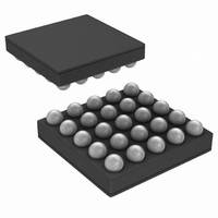
LM49101TM/NOPB National Semiconductor, LM49101TM/NOPB Datasheet - Page 5

LM49101TM/NOPB
Manufacturer Part Number
LM49101TM/NOPB
Description
IC AUDIO SUBSYSTM 1.3W AB 25USMD
Manufacturer
National Semiconductor
Series
Boomer®, PowerWise®r
Type
Class ABr
Datasheet
1.LM49101TMNOPB.pdf
(30 pages)
Specifications of LM49101TM/NOPB
Output Type
1-Channel (Mono) with Stereo Headphones
Max Output Power X Channels @ Load
1.3W x 1 @ 8 Ohm; 45mW x 2 @ 32 Ohm
Voltage - Supply
2.7 V ~ 5.5 V
Features
Depop, Differential Inputs, I²C, Shutdown, Thermal Protection, Volume Control
Mounting Type
Surface Mount
Package / Case
25-MicroSMD
Operational Class
Class-AB
Audio Amplifier Output Configuration
1-Channel Mono/2-Channel Stereo
Audio Amplifier Function
Headphone/Speaker
Single Supply Voltage (typ)
Not RequiredV
Dual Supply Voltage (typ)
3/5V
Power Supply Requirement
Triple
Rail/rail I/o Type
No
Power Supply Rejection Ratio
90dB
Single Supply Voltage (min)
Not RequiredV
Single Supply Voltage (max)
Not RequiredV
Dual Supply Voltage (min)
1.7/1.8/2.7V
Dual Supply Voltage (max)
2.9/5.5V
Operating Temp Range
-40C to 85C
Operating Temperature Classification
Industrial
Mounting
Surface Mount
Pin Count
25
Package Type
uSMD
Lead Free Status / RoHS Status
Lead free / RoHS Compliant
Other names
LM49101TMTR
I
I
V
P
DD
SD
Symbol
OS
O
Absolute Maximum Ratings
If Military/Aerospace specified devices are required,
please contact the National Semiconductor Sales Office/
Distributors for availability and specifications.
Electrical Characteristics V
The following specifications apply for V
specified. LS = Loudspeaker, HP = Headphone, EP = Earpiece.
Supply Voltage (Loudspeaker,
V
Supply Voltage (Headphone, V
Storage Temperature
Voltage at Any Input Pin
Power Dissipation (Note 3)
ESD Rating (Note 4)
ESD Rating (Note 5)
Junction Temperature (T
Soldering Information
DD
Vapor Phase (60sec.)
Infrared (15sec.)
LS)
Quiescent Power Supply Current
Shutdown Current
Output Offset Voltage
Output Power
Parameter
JMAX
)
DD
HP)
GND − 0.3 to V
DD
LS = 3.3V, V
−65°C to +150°C
Internally Limited
V
EP Receiver
(Output Mode Bit EP Bypass = 1)
LS only (Mode 1), GAMP_SD = 0
LS only (Mode 1), GAMP_SD = 1
HP only (Mode 8), GAMP_SD = 0
HP only (Mode 8), GAMP_SD = 1
LS+HP (Mode 10), GAMP_SD = 0
Power_On = 0
V
LS output, R
HP output, R
LS output, Mode 1, R
THD+N = 1%, f = 1kHz, LS_Gain = 6dB
HP output, Mode 8, R
THD+N = 1%, f = 1kHz
DD
IN
IN
(Notes 1, 2)
VDDLS
VDDHP
VDDLS
VDDHP
VDDLS
VDDHP
VDDLS +VDDHP
VDDLS
VDDHP
VDDLS
VDDHP
VDDLS +VDDHP
DD
= 0, No Load
= 0V, Mode 10
LS = 3.3V, V
LS + 0.3
2000V
150°C
215°C
220°C
DD
200V
6.0V
3.0V
HP = 2.75V, T
L
L
= 8Ω BTL
= 32Ω SE
Conditions
5
L
L
Operating Ratings
= 8Ω BTL
See AN-1112 “Micro SMD Wafer Level Chip Scale
Package”
Thermal Resistance
θ
Temperature Range
Supply Voltage (V
Supply Voltage (V
Supply Voltage (V
Supply Voltage (I
= 32Ω SE
DD
A
T
JA
MIN
= 25°C, all volume controls set to 0dB, unless otherwise
HP = 2.75V
(Note 8)
≤
T
A
≤
T
MAX
2
DD
DD
DD
CV
LS)
HP)
CP)
DD
(Note 6)
Typical
)
(Notes 1, 2)
0.03
0.01
540
2.5
1.6
3.1
2.8
3.3
2.8
3.1
2.5
0.5
44
0
2
0
LM49101
(Note 7)
Limits
0.045
6.45
480
4.2
2.0
4.5
3.8
4.5
1.8V
1.7V
22
40
2.7V
8
2
5
−40°C
V
V
I
≤
≤
2
DD
≤
DD
CV
V
I
V
CP = V
2
≤
DD
HP
CV
DD
DD
www.national.com
T
HP
LS
mA (max)
mA (max)
mA (max)
mA (max)
mA (max)
mA (max)
mA (max)
mA (max)
mV (max)
mV (max)
mW (min)
mW (min)
µA (max)
DD
A
(Limits)
≤
≤
51°C/W
Units
≤
≤
≤
V
≤
V
mA
mA
mA
mA
mA
DD
85°C
DD
DD
5.5V
2.9V
5.5V
HP
LS
LS


