LM49101TM/NOPB National Semiconductor, LM49101TM/NOPB Datasheet
LM49101TM/NOPB
Specifications of LM49101TM/NOPB


Related parts for LM49101TM/NOPB

LM49101TM/NOPB Summary of contents
Page 1
... Output power 5V 2.75V DD DD 1% THD+N = 8Ω speaker 32Ω headphone R L Boomer® registered trademark of National Semiconductor Corporation. © 2009 National Semiconductor Corporation LM49101 ■ Output Power 3.3V 1% THD+N = 8Ω speaker 32Ω headphone ...
Page 2
Typical Application www.national.com FIGURE 1. Typical Audio Application Circuit 2 30086203 ...
Page 3
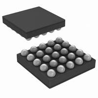
Connection Diagrams 25 Bump micro SMD Package Top View (Bump Side Down) Order Number LM49101TM, LM49101TMX See NS Package Number TMD25BCA Ordering Information Order Package Package DWG Number 25 Bump micro LM49101TM TMD25BCA SMD 25 Bump micro LM49101TMX TMD25BCA SMD ...
Page 4
Bump Descriptions Bump Name A1 CPGND Charge pump ground terminal Negative charge pump power supply SS A3 HPR Right headphone output Headphone amplifier power supply DD A5 MIN+ Positive input pin for the mono, ...
Page 5
... Absolute Maximum Ratings If Military/Aerospace specified devices are required, please contact the National Semiconductor Sales Office/ Distributors for availability and specifications. Supply Voltage (Loudspeaker, V LS) DD Supply Voltage (Headphone, V HP) DD Storage Temperature Voltage at Any Input Pin GND − 0 Power Dissipation (Note 3) ESD Rating (Note 4) ...
Page 6
Symbol Parameter THD+N Total Harmonic Distortion + Noise SNR Signal-to-Noise Ratio PSRR Power Supply Rejection Ratio CMRR Common-Mode Rejection Ratio X Crosstalk TALK Z MIN, LIN, and RIN Input Impedance Resistance ON VOL Digital Volume Control Range ...
Page 7
Electrical Characteristics V The following specifications apply for V specified Loudspeaker Headphone Earpiece. Symbol Parameter I Quiescent Power Supply Current DD I Shutdown Current SD V Output Offset Voltage OS P Output Power O ...
Page 8
Symbol Parameter CMRR Common-Mode Rejection Ratio X Crosstalk TALK Z MIN, LIN, and RIN Input Impedance Resistance ON VOL Digital Volume Control Range VOL Volume Control Step Size Error T Wake-Up Time from Shutdown WU www.national.com Conditions ...
Page 9
Interface 2. C_V The following specifications apply for V Symbol Parameter Clock Period Data Setup Time Data Stable Time 3 ...
Page 10
Typical Performance Characteristics THD+N vs Frequency = 8Ω BTL 3.3V Mode 1 (Mono), 80kHz BW THD+N vs Frequency 3.3V 1.8V 5mW/Ch, Mode ...
Page 11
THD+N vs Frequency = 8Ω BTL 5V Mode 1 (Mono), 80kHz BW THD+N vs Frequency 5V 2.75V 20mW/Ch, Mode 4 (Mono), ...
Page 12
THD+N vs Output Power 3.3V & 5V 1kHz Mode 1 (Mono), 80kHz BW THD+N vs Output Power 3.3V 1.8V & 2.75V 1kHz ...
Page 13
PSRR vs Frequency 3.3V 200mV , R DD RIPPLE PP Mode 1 (Mono), 80kHz BW PSRR vs Frequency 5V 200mV , R DD RIPPLE PP Mode 1 (Mono), ...
Page 14
PSRR vs Frequency 3.3V 2.75V 32Ω SE, Mode 4 (Mono), 80kHz Power Dissipation vs Output Power 3.3V & 5V 2.75V, R ...
Page 15
Supply Current vs Supply Voltage ( 2.75V, No Load, Gain_SD = 0 & (EP_Mode & 1, Mode 1 Supply Current vs Supply Voltage ( 3.3V, No Load, Gain_SD = ...
Page 16
Application Information COMPATIBLE INTERFACE The LM49101 is controlled through an I interface that consists of a serial data line (SDA) and a serial clock (SCL). The clock line is uni-directional. The data line is bi-directional (open drain). ...
Page 17
A7 A6 Chip 1 1 Address Register D7 D6 General Control 0 0 Output Mode Control 0 1 Bypass Output Gain Control 1 0 Mono Input Volume 1 0 Control Left Input Volume 1 1 Control Right Input Volume 1 ...
Page 18
Bit Name 0 Power_On 1 Turn_On_Time 3 LS (EP Mode) 4 GAMP_SD www.national.com TABLE 3. General Control Register Value This bit is a master shutdown control bit and sets the device off. Value 0 Master power ...
Page 19
TABLE 4. Output Mode Control Register (see key below table) Bits Field 3:0 Mode_Control These bits determine how the input signals are mixed and routed to the outputs Mode 0000 0001 0010 ...
Page 20
Bits Field 2:0 HP_GAIN 3 LS_GAIN 4 INPUT MUTE www.national.com TABLE 5. Output Gain Control Register Description These bits set the gain of the headphone output amplifiers. Value 000 001 010 011 100 101 110 111 This bit sets the ...
Page 21
TABLE 6. Input Volume Control Registers Bits Fields 4:0 Mono_Vol These bits set the input volume for each input volume register listed. Right_Vol Left_Vol Description Volume Step Value 1 00000 2 00001 3 00010 4 00011 5 00100 6 00101 ...
Page 22
HW RESET FUNCTION The LM49101 can be globally reset without using the I trols. When the HW RESET pin is set to a logic low the LM49101 will enter into shutdown, the mode control bits of the Output Mode Control ...
Page 23
DIFFERENTIAL AMPLIFIER EXPLANATION The LM49101 features a differential input stage, which offers improved noise rejection compared to a single-ended input amplifier. Because a differential input amplifier amplifies the difference between the two input signals, any component common to both signals ...
Page 24
Capacitors with a tolerance of 10% or better are recommend- ed for impedance matching and improved CMRR and PSRR. CHARGE PUMP FLYING CAPACITOR (C The flying capacitor (C ), see Figure 1, affects the load regu- 1 lation and output ...
Page 25
Demo Board Circuit Demonstration Board The demonstration board (see Figure 5) has connection and jumper options to be powered partially from the USB bus or from external power supplies. Additional options are to power the logic and ...
Page 26
LM49101 microSMD Demo Board Views Composite View Top Layer Internal Layer 2 www.national.com 30086209 30086206 30086207 26 30086205 Silk Screen 30086208 Internal Layer 1 30086210 Bottom Layer ...
Page 27
LM49101 Reference Demo Board Bill Of Materials Designator Vlaue Tolerance 5.1kΩ 10Ω 100kΩ IN1 IN2 1μF 10 IN3 IN4 ...
Page 28
Revision History Rev Date 0.01 10/18/08 www.national.com Description Initial released. 28 ...
Page 29
Physical Dimensions inches (millimeters) unless otherwise noted X = 2.040±0.030mm Bump micro SMD Package NS Package Number TMD25BCA = 2.066±0.030mm 0.600±0.075mm www.national.com ...
Page 30
... For more National Semiconductor product information and proven design tools, visit the following Web sites at: Products Amplifiers www.national.com/amplifiers Audio www.national.com/audio Clock and Timing www.national.com/timing Data Converters www.national.com/adc Interface www.national.com/interface LVDS www.national.com/lvds Power Management www.national.com/power Switching Regulators www.national.com/switchers LDOs www.national.com/ldo LED Lighting www ...