LM49101TM/NOPB National Semiconductor, LM49101TM/NOPB Datasheet - Page 24
LM49101TM/NOPB
Manufacturer Part Number
LM49101TM/NOPB
Description
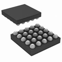
IC AUDIO SUBSYSTM 1.3W AB 25USMD
Manufacturer
National Semiconductor
Series
Boomer®, PowerWise®r
Type
Class ABr
Datasheet
1.LM49101TMNOPB.pdf
(30 pages)
Specifications of LM49101TM/NOPB
Output Type
1-Channel (Mono) with Stereo Headphones
Max Output Power X Channels @ Load
1.3W x 1 @ 8 Ohm; 45mW x 2 @ 32 Ohm
Voltage - Supply
2.7 V ~ 5.5 V
Features
Depop, Differential Inputs, I²C, Shutdown, Thermal Protection, Volume Control
Mounting Type
Surface Mount
Package / Case
25-MicroSMD
Operational Class
Class-AB
Audio Amplifier Output Configuration
1-Channel Mono/2-Channel Stereo
Audio Amplifier Function
Headphone/Speaker
Single Supply Voltage (typ)
Not RequiredV
Dual Supply Voltage (typ)
3/5V
Power Supply Requirement
Triple
Rail/rail I/o Type
No
Power Supply Rejection Ratio
90dB
Single Supply Voltage (min)
Not RequiredV
Single Supply Voltage (max)
Not RequiredV
Dual Supply Voltage (min)
1.7/1.8/2.7V
Dual Supply Voltage (max)
2.9/5.5V
Operating Temp Range
-40C to 85C
Operating Temperature Classification
Industrial
Mounting
Surface Mount
Pin Count
25
Package Type
uSMD
Lead Free Status / RoHS Status
Lead free / RoHS Compliant
Other names
LM49101TMTR


www.national.com
Capacitors with a tolerance of 10% or better are recommend-
ed for impedance matching and improved CMRR and PSRR.
CHARGE PUMP FLYING CAPACITOR (C
The flying capacitor (C
lation and output impedance of the charge pump. A C
that is too low results in a loss of current drive, leading to a
loss of amplifier headroom. A higher valued C
regulation and lowers charge pump output impedance to an
extent. Above 2.2μF, the R
and the ESR of C
A lower value capacitor can be used in systems with low max-
imum output power requirements.
CHARGE PUMP HOLD CAPACITOR (C
The value and ESR of the hold capacitor C
the ripple on V
put ripple. Decreasing the ESR of C
ripple and charge pump output impedance. A lower value ca-
pacitor can be used in systems with low maximum output
power requirements.
SELECTION OF INPUT RESISTORS
The Bypass_In inputs connect to the loudspeaker output
through an FET switch when EP Bypass is active (see Figure
5). Because THD through this path is mainly dominated by
the switch impedance variation, adding input resistors (R
R
improved THD. For example, a change in the switch
impedance from 2Ω to 3Ω is a 67% change in impedance. If
10Ω input resistors are used then the impedance change is
from 12Ω to 13Ω, only 7.7% impedance variation. The analog
switch impedance is typically 2Ω to 3.4Ω. The switch
impedance change is a result of heating and the increase in
R
The value of the input resistors must be balanced against the
amount of output current and the load impedance on the loud-
speaker outputs. A higher value input resistor reduces the
effects of switch impedance variation but also causes voltage
4
DS(ON)
in Figure 5) will help reduce impedance effects resulting in
of the FETs.
SS
CP. Increasing the value of C
1
and C
1
), see Figure 1, affects the load regu-
s3
DS(ON)
dominate the output impedance.
of the charge pump switches
s3
reduces both output
S3
1
)
s3
)
1
s3
directly affects
improves load
reduces out-
1
value
3
and
24
drop and reduced power to the load on the loudspeaker out-
puts.
The current through the FET switch should not exceed 500mA
or die heating may cause thermal shut down activation and
potential IC damage.
MINIMUM POWER OPERATION
The LM49101 has several options to reduce power consump-
tion and is designed to conserve power when possible. When
a speaker only mode is selected the headphone sections are
shutdown and the current drawn from the V
power supply will be zero. When a headphone mode is se-
lected the current drawn from the V
duced by shutting down unused circuitry. See the various
Supply Current vs Supply Voltage graphs in the Typical Per-
formance Characteristics section.
To reduce power consumption further, the additional control
bits GAMP_SD, LS (EP Mode), and HPR_SD are provided.
When low power consumption is more important than the
THD performance of the loudspeaker the LS (EP_mode) bit
should be set to '1' saving approximately 0.5mA from the
V
approximately 0.4mA for each input shut down. For modes
where only the mono input is used, up to 0.8mA can be saved
from the V
shut down the right headphone channel reducing power con-
sumption when only one amplifier headphone output is need-
ed.
Additionally, the supply voltages for the different V
(V
needed values to obtain the output power levels required by
the design. By reducing the supply voltage the total power
consumption will be reduced.
For best system efficiency, a DC-DC converter (buck) can be
used to power the V
V
achieve much higher efficiency (> 90%) than even a low
dropout regulator (LDO).
DD
DD
DD
LS supply. The GAMP_SD bit should be set on to save
LS supply instead of a linear regulator. DC-DC converters
LS, V
DD
DD
LS supply. Also, the HPR_SD bit can be used to
HP, and V
DD
DD
HP and V
CP) can be set to the minimum
DD
DD
CP voltages from the
LS supply is also re-
DD
HP/V
DD
DD
pins
CP
Related parts for LM49101TM/NOPB
Image
Part Number
Description
Manufacturer
Datasheet
Request
R

Part Number:
Description:
National Semiconductor [8-Bit D/A Converter]
Manufacturer:
National Semiconductor
Datasheet:
Part Number:
Description:
National Semiconductor [Media Coprocessor]
Manufacturer:
National Semiconductor
Datasheet:
Part Number:
Description:
Digitally Controlled Tone and Volume Circuit with Stereo Audio Power Amplifier, Microphone Preamp Stage and National 3D Sound
Manufacturer:
National Semiconductor
Datasheet:
Part Number:
Description:
Digitally Controlled Tone and Volume Circuit with Stereo Audio Power Amplifier, Microphone Preamp Stage and National 3D Sound
Manufacturer:
National Semiconductor
Datasheet:
Part Number:
Description:
AC97 Rev 2 Codec with Sample Rate Conversion and National 3D Sound
Manufacturer:
National Semiconductor
Part Number:
Description:
Manufacturer:
National Semiconductor
Datasheet:
Part Number:
Description:
Manufacturer:
National Semiconductor
Datasheet:
Part Number:
Description:
General Purpose, Low Voltage, Low Power, Rail-to-Rail Output Operational Amplifiers
Manufacturer:
National Semiconductor
Datasheet:
Part Number:
Description:
8-bit 20 MSPS flash A/D converter.
Manufacturer:
National Semiconductor
Datasheet:
Part Number:
Description:
Low Noise Quad Operational Amplifier
Manufacturer:
National Semiconductor
Datasheet:
Part Number:
Description:
Quad Differential Line Receivers
Manufacturer:
National Semiconductor
Datasheet:
Part Number:
Description:
Quad High Speed Trapezoidal? Bus Transceiver
Manufacturer:
National Semiconductor
Datasheet:
Part Number:
Description:
Dual Line Receiver
Manufacturer:
National Semiconductor
Datasheet:
Part Number:
Description:
TTL to 10k ECL Level Translator with Latch
Manufacturer:
National Semiconductor
Datasheet: