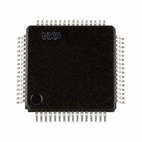
SC16C554IB64,151 NXP Semiconductors, SC16C554IB64,151 Datasheet - Page 15

SC16C554IB64,151
Manufacturer Part Number
SC16C554IB64,151
Description
IC UART QUAD SOT314-2
Manufacturer
NXP Semiconductors
Specifications of SC16C554IB64,151
Number Of Channels
4, QUART
Fifo's
16 Byte
Voltage - Supply
2.5V, 3.3V, 5V
With Auto Flow Control
Yes
With Irda Encoder/decoder
Yes
With False Start Bit Detection
Yes
With Modem Control
Yes
With Cmos
Yes
Mounting Type
Surface Mount
Package / Case
64-LQFP
Transmit Fifo
16Byte
Receive Fifo
16Byte
Transmitter And Receiver Fifo Counter
Yes
Data Rate
5Mbps
Package Type
LQFP
Operating Supply Voltage (max)
5.5V
Operating Supply Voltage (min)
4.5V
Mounting
Surface Mount
Operating Temperature (min)
-40C
Operating Temperature (max)
85C
Operating Temperature Classification
Industrial
Lead Free Status / RoHS Status
Lead free / RoHS Compliant
Other names
935270074151
SC16C554IB64-S
SC16C554IB64-S
SC16C554IB64-S
SC16C554IB64-S
Philips Semiconductors
9397 750 13132
Product data
6.4 Internal registers
6.5 FIFO operation
The SC16C554/554D provides 17 internal registers for monitoring and control. These
registers are shown in
(THR/RHR), interrupt status and control registers (IER/ISR), a FIFO control register
(FCR), line status and control registers (LCR/LSR), modem status and control
registers (MCR/MSR), programmable data rate (clock) control registers (DLL/DLM),
and a user accessible scratchpad register (SPR). Beyond the general 16C554
features and capabilities, the SC16C554/554D offers an enhanced feature register
set (EFR, Xon/Xoff1-2) that provides on-board hardware/software flow control.
Register functions are more fully described in the following paragraphs.
Table 5:
[1]
[2]
[3]
The 16 byte transmit and receive data FIFOs are enabled by the FIFO Control
Register (FCR) bit 0. With SC16C554 devices, the user can set the receive trigger
level, but not the transmit trigger level. The receiver FIFO section includes a time-out
function to ensure data is delivered to the external CPU. An interrupt is generated
whenever the Receive Holding Register (RHR) has not been read following the
loading of a character or the receive trigger level has not been reached.
A2
General register set (THR/RHR, IER/ISR, MCR/MSR, FCR, LSR, SPR)
0
0
0
0
1
1
1
1
Baud rate register set (DLL/DLM)
0
0
Enhanced register set (EFR, Xon/off 1-2)
0
1
1
1
1
These registers are accessible only when LCR[7] is a logic 0.
These registers are accessible only when LCR[7] is a logic 1.
Enhanced Feature Register, Xon1, 2 and Xoff1, 2 are accessible only when the LCR is set to
‘BF’ (HEX).
A1
0
0
1
1
0
0
1
1
0
0
1
0
0
1
1
Internal registers decoding
Quad UART with 16-byte FIFO and infrared (IrDA) encoder/decoder
A0
0
1
0
1
0
1
0
1
0
1
0
0
1
0
1
Rev. 05 — 10 May 2004
READ mode
Receive Holding Register
Interrupt Enable Register
Interrupt Status Register
Line Control Register
Modem Control Register
Line Status Register
Modem Status Register
Scratchpad Register
LSB of Divisor Latch
MSB of Divisor Latch
Enhanced Feature Register
Xon1 word
Xon2 word
Xoff1 word
Xoff2 word
Table
5. These registers function as data holding registers
[2]
[3]
SC16C554/554D
WRITE mode
Transmit Holding Register
Interrupt Enable Register
FIFO Control Register
Line Control Register
Modem Control Register
n/a
n/a
Scratchpad Register
LSB of Divisor Latch
MSB of Divisor Latch
Enhanced Feature Register
Xon1 word
Xon2 word
Xoff1 word
Xoff2 word
© Koninklijke Philips Electronics N.V. 2004. All rights reserved.
[1]
15 of 55


