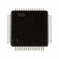
SC16C554IB64,151 NXP Semiconductors, SC16C554IB64,151 Datasheet - Page 10

SC16C554IB64,151
Manufacturer Part Number
SC16C554IB64,151
Description
IC UART QUAD SOT314-2
Manufacturer
NXP Semiconductors
Specifications of SC16C554IB64,151
Number Of Channels
4, QUART
Fifo's
16 Byte
Voltage - Supply
2.5V, 3.3V, 5V
With Auto Flow Control
Yes
With Irda Encoder/decoder
Yes
With False Start Bit Detection
Yes
With Modem Control
Yes
With Cmos
Yes
Mounting Type
Surface Mount
Package / Case
64-LQFP
Transmit Fifo
16Byte
Receive Fifo
16Byte
Transmitter And Receiver Fifo Counter
Yes
Data Rate
5Mbps
Package Type
LQFP
Operating Supply Voltage (max)
5.5V
Operating Supply Voltage (min)
4.5V
Mounting
Surface Mount
Operating Temperature (min)
-40C
Operating Temperature (max)
85C
Operating Temperature Classification
Industrial
Lead Free Status / RoHS Status
Lead free / RoHS Compliant
Other names
935270074151
SC16C554IB64-S
SC16C554IB64-S
SC16C554IB64-S
SC16C554IB64-S
Philips Semiconductors
Table 2:
9397 750 13132
Product data
Symbol
D0-D2,
D3-D7
DSRA,
DSRB,
DSRC, DSRD
DTRA,
DTRB,
DTRC, DTRD
GND
INTA, INTB,
INTC, INTD
INTSEL
IOR
Pin description
Pin
PLCC68 LQFP64 LQFP80
66-68,
1-5
10, 26,
44, 60
12, 24,
46, 58
6, 23,
40, 57
15, 21,
49, 55
65
52
53-55,
56-60
1, 17,
32, 48
3, 15,
34, 46
14, 28,
45, 61
6, 12,
37, 43
-
40
…continued
7-9,
11-15
22, 39,
62, 79
24, 37,
64, 77
16, 36,
56, 76
27, 34,
67, 74
6
70
Quad UART with 16-byte FIFO and infrared (IrDA) encoder/decoder
Type
I/O
I
O
I
O
I
I
Rev. 05 — 10 May 2004
Description
Data bus (bi-directional). These pins are the 8-bit, 3-State data bus
for transferring information to or from the controlling CPU. D0 is the
least significant bit and the first data bit in a transmit or receive serial
data stream.
Data Set Ready (Active-LOW). These inputs are associated with
individual UART channels, A through D. A logic 0 on this pin indicates
the modem or data set is powered-on and is ready for data exchange
with the UART. This pin has no effect on the UART’s transmit or
receive operation.
Data Terminal Ready (Active-LOW). These outputs are associated
with individual UART channels, A through D. A logic 0 on this pin
indicates that the SC16C554/554D is powered-on and ready. This pin
can be controlled via the modem control register. Writing a logic 1 to
MCR[0] will set the DTR output to logic 0, enabling the modem. This
pin will be a logic 1 after writing a logic 0 to MCR[0], or after a reset.
This pin has no effect on the UART’s transmit or receive operation.
Signal and power ground.
Interrupt A, B, C, D (Active-HIGH). This function is associated with
the 16 mode only. These pins provide individual channel interrupts
INTA-INTD. INTA-INTD are enabled when MCR[3] is set to a logic 1,
interrupts are enabled in the interrupt enable register (IER), and
when an interrupt condition exists. Interrupt conditions include:
receiver errors, available receiver buffer data, transmit buffer empty,
or when a modem status flag is detected. When the 68 mode is
selected, the functions of these pins are re-assigned. 68 mode
functions are described under their respective name/pin headings.
Interrupt Select (Active-HIGH, with internal pull-down). This
function is associated with the 16 mode only. When the 16 mode is
selected, this pin can be used in conjunction with MCR[3] to enable
or disable the 3-State interrupts, INTA-INTD, or override MCR[3] and
force continuous interrupts. Interrupt outputs are enabled
continuously by making this pin a logic 1. Making this pin a logic 0
allows MCR[3] to control the 3-State interrupt output. In this mode,
MCR[3] is set to a logic 1 to enable the 3-State outputs. This pin is
disabled in the 68 mode. Due to pin limitations on the 64-pin
packages, this pin is not available. To cover this limitation, the
SC16C654DIB64 version operates in the continuous interrupt enable
mode by bonding this pin to V
operates with MCR[3] control by bonding this pin to GND.
Input/Output Read strobe (Active-LOW). This function is
associated with the 16 mode only. A logic 0 transition on this pin will
load the contents of an internal register defined by address bits
A0-A2 onto the SC16C554/554D data bus (D0-D7) for access by
external CPU. This pin is disabled in the 68 mode.
CC
SC16C554/554D
internally. The SC16C654IB64
© Koninklijke Philips Electronics N.V. 2004. All rights reserved.
10 of 55


