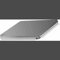
PC87393VJG National Semiconductor, PC87393VJG Datasheet - Page 59

PC87393VJG
Manufacturer Part Number
PC87393VJG
Description
IC, SUPER I/O DEVICE, TQFP-100
Manufacturer
National Semiconductor
Specifications of PC87393VJG
Data Rate
2Mbps
Supply Voltage Range
3V to 3.6V
Logic Case Style
TQFP
No. Of Pins
100
Operating Temperature Range
0°C to +70°C
Termination Type
SMD
Transceiver Type
Interface
Rohs Compliant
No
Available stocks
Company
Part Number
Manufacturer
Quantity
Price
Part Number:
PC87393VJG
Manufacturer:
NS/国半
Quantity:
20 000
- Current page: 59 of 148
- Download datasheet (2Mb)
2.0 Device Architecture and Configuration
2.15.5 GPIO Pin Configuration Register
This register reflects, for both read and write, the register currently selected by the GPIO Pin Select register. All the GPIO
Pin registers that are accessed via this register have a common bit structure, as shown below. This register is reset by hard-
ware to 44h, except for ports 2 and 3, that are reset to 04h, and GPIO36 which resets to 00h.
Location:
Type:
Ports: 0 and 1 (with event detection capability)
Ports 2 and 3 (without event detection capability)
Bit
Name
Reset
Bit
Name
Reset
Bit
7
6
5
4
3
Reserved
Event Debounce Enable. (Ports 0 and 1 with event detection capability). Enables transferring the signal only
after a predetermined debouncing period of time.
0: Disabled
1: Enabled (default)
Reserved. (Ports 2 and 3). Always 0.
Event Polarity. (Ports 0 and 1 with event detection capability). This bit defines the polarity of the signal that
issues an interrupt from the corresponding GPIO pin (falling/low or rising/high).
0: Falling edge or low level input (default)
1: Rising edge or high level input
Reserved. (Ports 2 and 3). Always 0.
Event Type. (Ports 0 and 1 with event detection capability). This bit defines the type of the signal that issues an
interrupt from the corresponding GPIO pin (edge or level).
0: Edge input (default)
1: Level input
Reserved. (Ports 2 and 3). Always 0.
Lock. This bit locks the corresponding GPIO pin. Once this bit is set to 1 by software, it can only be cleared to
0 by system reset or power-off. Pin multiplexing is functional until the Multiplexing Lock bit is 1 (bit 7 of SuperI/O
Configuration 1 register, SIOCF1).
0: No effect (default)
1: Direction, output type, pull-up and output value locked
Index F1h
R/W
Reserved
7
0
7
0
Debounce
Enable
Event
6
1
6
0
Reserved
Polarity
Event
5
0
5
0
Event Type
Description
59
4
0
4
0
(Continued)
Lock
Lock
3
0
3
0
Control
Control
Pull-Up
Pull-Up
2
1
2
1
Output
Output
Type
Type
1
0
1
0
www.national.com
Output
Enable
Output
Enable
0
0
0
0
Related parts for PC87393VJG
Image
Part Number
Description
Manufacturer
Datasheet
Request
R
Part Number:
Description:
National Semiconductor [8-Bit D/A Converter]
Manufacturer:
National Semiconductor
Datasheet:
Part Number:
Description:
National Semiconductor [Media Coprocessor]
Manufacturer:
National Semiconductor
Datasheet:
Part Number:
Description:
Digitally Controlled Tone and Volume Circuit with Stereo Audio Power Amplifier, Microphone Preamp Stage and National 3D Sound
Manufacturer:
National Semiconductor
Datasheet:
Part Number:
Description:
Digitally Controlled Tone and Volume Circuit with Stereo Audio Power Amplifier, Microphone Preamp Stage and National 3D Sound
Manufacturer:
National Semiconductor
Datasheet:
Part Number:
Description:
AC97 Rev 2 Codec with Sample Rate Conversion and National 3D Sound
Manufacturer:
National Semiconductor
Part Number:
Description:
Manufacturer:
National Semiconductor
Datasheet:
Part Number:
Description:
Manufacturer:
National Semiconductor
Datasheet:
Part Number:
Description:
General Purpose, Low Voltage, Low Power, Rail-to-Rail Output Operational Amplifiers
Manufacturer:
National Semiconductor
Datasheet:
Part Number:
Description:
8-bit 20 MSPS flash A/D converter.
Manufacturer:
National Semiconductor
Datasheet:
Part Number:
Description:
Low Noise Quad Operational Amplifier
Manufacturer:
National Semiconductor
Datasheet:
Part Number:
Description:
Quad Differential Line Receivers
Manufacturer:
National Semiconductor
Datasheet:
Part Number:
Description:
Quad High Speed Trapezoidal? Bus Transceiver
Manufacturer:
National Semiconductor
Datasheet:
Part Number:
Description:
Dual Line Receiver
Manufacturer:
National Semiconductor
Datasheet:
Part Number:
Description:
TTL to 10k ECL Level Translator with Latch
Manufacturer:
National Semiconductor
Datasheet:


