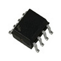
FM93C46EM8X Fairchild Semiconductor, FM93C46EM8X Datasheet - Page 7

FM93C46EM8X
Manufacturer Part Number
FM93C46EM8X
Description
Manufacturer
Fairchild Semiconductor
Datasheet
1.FM93C46EM8X.pdf
(13 pages)
Specifications of FM93C46EM8X
Density
1Kb
Interface Type
Serial (Microwire)
Organization
64x16
Frequency (max)
1MHz
Write Protection
Yes
Data Retention
40Year
Operating Supply Voltage (typ)
5V
Package Type
SOIC N
Operating Temp Range
-40C to 85C
Supply Current
1mA
Operating Supply Voltage (min)
4.5V
Operating Supply Voltage (max)
5.5V
Operating Temperature Classification
Industrial
Mounting
Surface Mount
Pin Count
8
Lead Free Status / Rohs Status
Compliant
Available stocks
Company
Part Number
Manufacturer
Quantity
Price
Company:
Part Number:
FM93C46EM8X
Manufacturer:
EPCOS
Quantity:
3 718
Part Number:
FM93C46EM8X
Manufacturer:
FAIRCHILD/仙童
Quantity:
20 000
FM93C46 Rev. D.1
The Erase all instruction will program all locations to a logical “1”
state. Input information (Start bit, Opcode and Address) for this
WDS instruction should be issued as listed under Table1. After
inputting the last bit of data (A0 bit), CS signal must be brought low
before the next rising edge of the SK clock. This falling edge of the
CS initiates the self-timed programming cycle. It takes t
(Refer appropriate DC and AC Electrical Characteristics table) for
the internal programming cycle to finish. During this time, the
device remains busy and is not ready for another instruction.
Status of the internal programming can be polled as described
under WRITE instruction description. While the device is busy, it
is recommended that no new instruction be issued. Refer Erase
All cycle diagram.
instruction prior to the “WRITE” or “WRITE ALL” instruction, respectively. The
“ERASE” and “ERASE ALL” instructions are included to maintain compatibility with
earlier technology EEPROMs.Clearing of Ready/Busy status
When programming is in progress, the Data-Out pin will display
The Fairchild CMOS EEPROMs do not require an “ERASE” or “ERASE ALL”
WP
time
the programming status as either BUSY (low) or READY (high)
when CS is brought high (DO output will be tri-stated when CS is
low). To restate, during programming, the CS pin may be brought
high and low any number of times to view the programming status
without affecting the programming operation. Once programming
is completed (Output in READY state), the output is ‘cleared’
(returned to normal tri-state condition) by clocking in a Start Bit.
After the Start Bit is clocked in, the output will return to a tri-stated
condition. When clocked in, this Start Bit can be the first bit in a
command string, or CS can be brought low again to reset all
internal circuits. Refer Clearing Ready Status diagram.
Application Note: AN758 - Using Fairchild’s MICROWIRE™ EE-
PROM.
www.fairchildsemi.com


