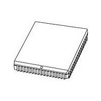
P80C592FFA NXP Semiconductors, P80C592FFA Datasheet - Page 82

P80C592FFA
Manufacturer Part Number
P80C592FFA
Description
Manufacturer
NXP Semiconductors
Datasheet
1.P80C592FFA.pdf
(108 pages)
Specifications of P80C592FFA
Cpu Family
80C
Device Core
80C51
Device Core Size
8b
Frequency (max)
16MHz
Interface Type
CAN/UART
Program Memory Type
ROMLess
Program Memory Size
Not Required
Total Internal Ram Size
512Byte
# I/os (max)
40
Number Of Timers - General Purpose
3
Operating Supply Voltage (typ)
5V
Operating Supply Voltage (max)
5.5V
Operating Supply Voltage (min)
4.5V
On-chip Adc
8-chx10-bit
Instruction Set Architecture
CISC
Operating Temp Range
-40C to 85C
Operating Temperature Classification
Industrial
Mounting
Surface Mount
Pin Count
68
Package Type
PLCC
Lead Free Status / Rohs Status
Compliant
Available stocks
Company
Part Number
Manufacturer
Quantity
Price
Company:
Part Number:
P80C592FFA
Manufacturer:
PANASONIC
Quantity:
1 200
Part Number:
P80C592FFA
Manufacturer:
PHI
Quantity:
20 000
Company:
Part Number:
P80C592FFA/00
Manufacturer:
SYSTECH
Quantity:
40
Part Number:
P80C592FFA/00
Manufacturer:
NXP/恩智浦
Quantity:
20 000
Company:
Part Number:
P80C592FFA/00,512
Manufacturer:
ON
Quantity:
300
Company:
Part Number:
P80C592FFA/00,512
Manufacturer:
NXP Semiconductors
Quantity:
10 000
Company:
Part Number:
P80C592FFA/00,518
Manufacturer:
NXP Semiconductors
Quantity:
10 000
Company:
Part Number:
P80C592FFA/00Ј¬512
Manufacturer:
NXP
Quantity:
702
Philips Semiconductors
Notes to the DC characteristics
1. Conditions for:
2. Conditions for:
3. Conditions for:
4. Window devices have to be covered. Conditions for:
5. Capacitive loads on Port 0 and Port 2 may degrade the LOW level output voltage of ALE, Port 1 and Port 3.
1996 Jun 27
SYMBOL
CAN output driver (V
V
V
Reference (AV
V
I
REFIN
OLT
OHT
REFOUT
8-bit microcontroller with on-chip CAN
a) The digital operating current measurement: all output pins disconnected; XTAL1 is driven with t
b) The analog operating current measurement: Port 5 = AV
a) The digital Idle mode supply current measurement: all output pins disconnected;
b) The analog Idle mode current measurement: Port 5 = AV
a) The digital Idle and Sleep mode supply current measurement: all output pins disconnected;
b) The analog Idle and Sleep mode current measurement: Port 5 = AV
a) The digital Power-down mode supply current measurement: all output pins and Port 5 disconnected;
b) The analog Power-down mode supply current measurement: Port 5 = AV
During a HIGH-to-LOW transition on the Port 0 and Port 2 pins and a capacitive load 100 pF, the ALE LOW level
may exceed 0.8 V. In the case that it is necessary to connect ALE to a Schmitt trigger input respectively use an
address latch with a Schmitt trigger STROBE input.
V
STADC = V
load current reference voltage source 100 A.
XTAL1 is driven with t
EA = RST = STADC = V
load current reference voltage source 100 A.
XTAL1 is driven with t
Port 0 = P1.6 = P1.7 = EW = CRX0 = V
CAN: register 6: = 00H, register 7: = 12H, register 8: = 02H, register 0: = 20H, wait 15t
register 1: = 10H, wait for bit Sleep = 1.
load current reference voltage source 100 A.
Port 0 = P1.6 = P1.7 = EW = CRX0 = V
AV
EA = RST = STADC = CRX1 = XTAL1 = AV
IL
DD
= V
LOW level output voltage
(CTX0 and CTX1)
High level output voltage
(CTX0 and CTX1)
REF output voltage
REF input current
= V
SS
DD
DD
+ 0.5 V; V
SS
= 5 V
, but current into AV
; CRX0 = 2.7 V; CRX1 = 2.3 V.
DD
PARAMETER
= 5 V
IH
5%)
r
r
= V
= t
= t
SS
f
f
DD
= 10 ns; V
; CRX0 = 2.7 V; CRX1 = 2.3 V.
= 10 ns; V
5%)
0.5 V; EA = RST = Port 0 = P1.6 = P1.7 = EW = V
DD
pin is not comprised in digital Power-down current.
IL
IL
= V
= V
DD
DD
; EA = RST = STADC = CRX1 = V
;
SS
SS
I
I
I
I
C
bit Reference Active = HIGH
1.5 V
bit Reference Active = LOW
o
o
o
o
0.1 mA
REF+
L
= 1.2 mA; note 15
= 10 mA
= 1.2 mA; note 15
= 10 mA; note 16
+ 0.5 V; V
+ 0.5 V; V
= 10 nF; note 15;
= AV
82
V
CONDITIONS
REFIN
I
L
REF
IH
IH
DD
DD
= V
= V
0.1 mA;
; CAN: register 6: = 00H;
= CV
; CAN: register 6: = 00H;
AV
DD
DD
DD
SS
0.5 V; Port 0 = P1.6 = P1.7 = EW = V
0.5 V;
1.5 V;
= V
DD
;
SS
;
DD
V
V
1
.
SS
2
DD
DD
AV
;
MIN.
DD
DD
0.6
0.1
;
0.1
CY
,
0.1
0.6
1
Product specification
10
2
AV
MAX.
P8xC592
DD
r
= t
+0.1
f
= 10 ns;
DD
V
V
V
V
V
UNIT
;
A


