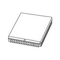
P80C592FFA NXP Semiconductors, P80C592FFA Datasheet - Page 47

P80C592FFA
Manufacturer Part Number
P80C592FFA
Description
Manufacturer
NXP Semiconductors
Datasheet
1.P80C592FFA.pdf
(108 pages)
Specifications of P80C592FFA
Cpu Family
80C
Device Core
80C51
Device Core Size
8b
Frequency (max)
16MHz
Interface Type
CAN/UART
Program Memory Type
ROMLess
Program Memory Size
Not Required
Total Internal Ram Size
512Byte
# I/os (max)
40
Number Of Timers - General Purpose
3
Operating Supply Voltage (typ)
5V
Operating Supply Voltage (max)
5.5V
Operating Supply Voltage (min)
4.5V
On-chip Adc
8-chx10-bit
Instruction Set Architecture
CISC
Operating Temp Range
-40C to 85C
Operating Temperature Classification
Industrial
Mounting
Surface Mount
Pin Count
68
Package Type
PLCC
Lead Free Status / Rohs Status
Compliant
Available stocks
Company
Part Number
Manufacturer
Quantity
Price
Company:
Part Number:
P80C592FFA
Manufacturer:
PANASONIC
Quantity:
1 200
Part Number:
P80C592FFA
Manufacturer:
PHI
Quantity:
20 000
Company:
Part Number:
P80C592FFA/00
Manufacturer:
SYSTECH
Quantity:
40
Part Number:
P80C592FFA/00
Manufacturer:
NXP/恩智浦
Quantity:
20 000
Company:
Part Number:
P80C592FFA/00,512
Manufacturer:
ON
Quantity:
300
Company:
Part Number:
P80C592FFA/00,512
Manufacturer:
NXP Semiconductors
Quantity:
10 000
Company:
Part Number:
P80C592FFA/00,518
Manufacturer:
NXP Semiconductors
Quantity:
10 000
Company:
Part Number:
P80C592FFA/00Ј¬512
Manufacturer:
NXP
Quantity:
702
Philips Semiconductors
Table 57 Description of the other DSCR2 bits
13.5.13.2 Data Field
The number of transferred data bytes is determined by the
Data Length Code. The first bit transmitted is the most
significant bit of data byte 1 at address 12.
13.5.14 R
The layout of the Receive Buffer and the individual bytes
correspond to the definitions given for the Transmit Buffer
layout, except that the addresses start at 20 instead of 10
(see Fig.15).
Table 58 The SFRs between CPU and CAN
Reserved bits are read as HIGH. R = Read; W = Write; R/W = Read/Write.
1996 Jun 27
BIT SYMBOL
CANADR
DBH
CANDAT
DAH
CANCON; Do not use a RMW instruction
D9H
CANSTA; The bit addresses of CANSTA (7 to 0) are DFH to D8H; do not use a RMW instruction
DFH to D8H R
ADDRESS
4
3
2
1
0
8-bit microcontroller with on-chip CAN
RTR
DLC.3
DLC.2
DLC.1
DLC.0
ECEIVE
ACCESS
R/W
R/W
R
W
W
Remote Transmission Request. If the RTR bit is:
Data Length Code (DLC). The number of bytes (Data Byte Count) in the Data Field of a message is
coded by the Data Length Code. At the start of a Remote Frame transmission the Data Length Code
is not considered due to the RTR bit being HIGH (remote). This forces the number of
transmitted/received data bytes to be a logic 0. Nevertheless, the Data Length Code must be
specified correctly to avoid bus errors, if two CAN-controllers start a Remote Frame transmission
simultaneously. The range of the Data Byte Count is 0 to 8 bytes and coded as follows:
For reasons of compatibility no Data Byte Counts other than 0,1,2,....8 should be used.
B
UFFER LAYOUT
Data Byte Count
HIGH (remote), then the Remote Frame will be transmitted by the CAN-controller.
LOW (data), then the Data Frame will be transmitted by the CAN-controller.
DMA
CAND7
Reserved Reserved Reserved WUI
RX0A
BS
RAMA7
7
=
Reserved AutoInc
CAND6
RX1A
ES
RAMA6
8DLC.3
6
+
CAND5
WUM
TS
RAMA5
4DLC.2
5
+
47
2DLC.1
13.5.15 H
Via the four special registers CANADR, CANDAT,
CANCON and CANSTA the CPU has access to the
CAN-controller and also to the DMA-logic. Note that
CANCON and CANSTA have different meanings for a
Read and Write access.
CANA4
CAND4
SLP
RS
RAMA4
FUNCTION
4
+
DLC.0
BIT
ANDLING OF THE
CANA3
CAND3
OI
COS
TCS
RAMA3
.
3
CANA2
CAND2
EI
RRB
TBS
RAMA2
CPU-CAN
2
CANA1
CAND1
TI
AT
DO
RAMA1
Product specification
INTERFACE
1
P8xC592
CANA0
CAND0
RI
TR
RBS
RAMA0
0


