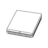
P80C592FFA NXP Semiconductors, P80C592FFA Datasheet - Page 30

P80C592FFA
Manufacturer Part Number
P80C592FFA
Description
Manufacturer
NXP Semiconductors
Datasheet
1.P80C592FFA.pdf
(108 pages)
Specifications of P80C592FFA
Cpu Family
80C
Device Core
80C51
Device Core Size
8b
Frequency (max)
16MHz
Interface Type
CAN/UART
Program Memory Type
ROMLess
Program Memory Size
Not Required
Total Internal Ram Size
512Byte
# I/os (max)
40
Number Of Timers - General Purpose
3
Operating Supply Voltage (typ)
5V
Operating Supply Voltage (max)
5.5V
Operating Supply Voltage (min)
4.5V
On-chip Adc
8-chx10-bit
Instruction Set Architecture
CISC
Operating Temp Range
-40C to 85C
Operating Temperature Classification
Industrial
Mounting
Surface Mount
Pin Count
68
Package Type
PLCC
Lead Free Status / Rohs Status
Compliant
Available stocks
Company
Part Number
Manufacturer
Quantity
Price
Company:
Part Number:
P80C592FFA
Manufacturer:
PANASONIC
Quantity:
1 200
Part Number:
P80C592FFA
Manufacturer:
PHI
Quantity:
20 000
Company:
Part Number:
P80C592FFA/00
Manufacturer:
SYSTECH
Quantity:
40
Part Number:
P80C592FFA/00
Manufacturer:
NXP/恩智浦
Quantity:
20 000
Company:
Part Number:
P80C592FFA/00,512
Manufacturer:
ON
Quantity:
300
Company:
Part Number:
P80C592FFA/00,512
Manufacturer:
NXP Semiconductors
Quantity:
10 000
Company:
Part Number:
P80C592FFA/00,518
Manufacturer:
NXP Semiconductors
Quantity:
10 000
Company:
Part Number:
P80C592FFA/00Ј¬512
Manufacturer:
NXP
Quantity:
702
Philips Semiconductors
13.5
The CAN-controller appears to the CPU as a
memory-mapped peripheral, guaranteeing the
independent operation of both parts.
13.5.1
The address area of the CAN-controller consists of the
Control Segment and the message buffers. The Control
Segment is programmed during an initialization down-load
in order to configure communication parameters (e.g. bit
timing). The communication over the CAN-bus is also
controlled via this segment by the CPU. A message which
is to be transmitted, must be written to the Transmit Buffer.
1996 Jun 27
handbook, full pagewidth
8-bit microcontroller with on-chip CAN
Control Segment and Message Buffer
description
1AH
1BH
1CH
1DH
0CH
0DH
11H
12H
13H
14H
15H
16H
17H
18H
19H
0AH
0BH
0EH
A
00H
0FH
10H
ADDRESS
01H
02H
03H
04H
05H
06H
07H
08H
09H
DDRESS ALLOCATION
10
11
12
13
14
15
16
17
18
19
20
21
22
23
24
25
26
27
28
29
0
1
2
3
4
5
6
7
8
9
CONTROL
COMMAND
STATUS
INTERRUPT
ACCEPTANCE CODE
ACCEPTANCE MASK
BUS TIMING 0
BUS TIMING 1
OUTPUT CONTROL
TEST
IDENTIFIER,
RTR BIT,
BYTE 1
BYTE 2
BYTE 3
BYTE 4
BYTE 5
BYTE 6
BYTE 7
BYTE 8
IDENTIFIER,
RTR BIT,
BYTE 1
BYTE 2
BYTE 3
BYTE 4
BYTE 5
BYTE 6
BYTE 7
BYTE 8
DATA LENGTH CODE
DATA LENGTH CODE
Fig.15 CAN-controller internal address allocation.
control segment
data field
descriptor
IDENTIFIER,
RTR BIT,
BYTE 1
BYTE 2
BYTE 3
BYTE 4
BYTE 5
BYTE 6
BYTE 7
BYTE 8
30
After a successful reception the CPU may read the
message from the Receive Buffer and then release it for
further use.
13.5.2
The exchange of status, control and command signals
between the CPU and the CAN-controller is performed in
the control segment. The layout of this segment is shown
in Fig.15. After an initial down-load, the contents of the
registers Acceptance Code, Acceptance Mask,
Bus Timing 0, Bus Timing 1 and Output Control should not
be changed. These registers may only be accessed when
the Reset Request bit in the Control Register is set HIGH
(see Tables 30, 31 and 32).
transmit buffer
DATA LENGTH CODE
C
ONTROL
S
EGMENT LAYOUT
data field
descriptor
MGA160 - 1
Product specification
receive buffer 0 or 1
P8xC592


