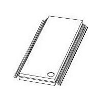
PCF8576DT NXP Semiconductors, PCF8576DT Datasheet - Page 8

PCF8576DT
Manufacturer Part Number
PCF8576DT
Description
Manufacturer
NXP Semiconductors
Datasheet
1.PCF8576DT.pdf
(52 pages)
Specifications of PCF8576DT
Operating Supply Voltage (typ)
2.5/3.3/5V
Number Of Digits
20
Number Of Segments
160
Package Type
TSSOP
Pin Count
56
Mounting
Surface Mount
Power Dissipation
400mW
Frequency (max)
400KHz
Operating Supply Voltage (min)
1.8V
Operating Supply Voltage (max)
5.5V
Lead Free Status / Rohs Status
Supplier Unconfirmed
Available stocks
Company
Part Number
Manufacturer
Quantity
Price
Part Number:
PCF8576DT
Manufacturer:
NXP/恩智浦
Quantity:
20 000
Part Number:
PCF8576DT/2
Manufacturer:
NXP/恩智浦
Quantity:
20 000
NXP Semiconductors
PCF8576D_9
Product data sheet
7.1 Power-on reset
7.2 LCD bias generator
The host microprocessor or microcontroller maintains the 2-line I
channel with the PCF8576D. The internal oscillator is enabled by connecting
pin OSC to pin V
are generated internally. The only other connections required to complete the system are
to the power supplies (V
At power-on the PCF8576D resets to the following starting conditions:
Data transfers on the I
reset action to complete.
Fractional LCD biasing voltages are obtained from an internal voltage divider consisting of
three impedances connected in series between V
bypassed to provide a
voltage can be temperature compensated externally using the supply to pin V
Fig 5.
•
•
•
•
•
•
•
•
All backplane outputs are set to V
All segment outputs are set to V
The selected drive mode is: 1:4 multiplex with
Blinking is switched off
Input and output bank selectors are reset
The I
The data pointer and the subaddress counter are cleared (set to logic 0)
Display is disabled
V
V
SS
DD
CONTROLLER
PROCESSOR/
2
The resistance of the power lines must be kept to a minimum.
For chip-on-glass applications, due to the Indium Tin Oxide (ITO) track resistance, each supply line
must be routed separately between the chip and the connector.
Typical system configuration
C-bus interface is initialized
MICRO-
MICRO-
HOST
R
SS
2C
. The appropriate biasing voltages for the multiplexed LCD waveforms
t
r
B
2
Rev. 09 — 25 August 2009
1
C-bus must be avoided for 1 ms following power-on to allow the
2
DD
bias voltage level for the 1:2 multiplex configuration. The LCD
, V
SS
and V
OSC
SDA
SCL
LCD
LCD
LCD
A0
) and the LCD panel chosen for the application.
Universal LCD driver for low multiplex rates
PCF8576D
A1
V
DD
A2
V
LCD
LCD
1
SA0
3
bias
and V
V
SS
40 segment drives
4 backplanes
SS
. The middle resistor can be
2
C-bus communication
PCF8576D
© NXP B.V. 2009. All rights reserved.
LCD PANEL
(up to 160
elements)
mdb079
LCD
.
8 of 52


