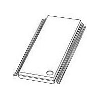
PCF8576DT NXP Semiconductors, PCF8576DT Datasheet - Page 22

PCF8576DT
Manufacturer Part Number
PCF8576DT
Description
Manufacturer
NXP Semiconductors
Datasheet
1.PCF8576DT.pdf
(52 pages)
Specifications of PCF8576DT
Operating Supply Voltage (typ)
2.5/3.3/5V
Number Of Digits
20
Number Of Segments
160
Package Type
TSSOP
Pin Count
56
Mounting
Surface Mount
Power Dissipation
400mW
Frequency (max)
400KHz
Operating Supply Voltage (min)
1.8V
Operating Supply Voltage (max)
5.5V
Lead Free Status / Rohs Status
Supplier Unconfirmed
Available stocks
Company
Part Number
Manufacturer
Quantity
Price
Part Number:
PCF8576DT
Manufacturer:
NXP/恩智浦
Quantity:
20 000
Part Number:
PCF8576DT/2
Manufacturer:
NXP/恩智浦
Quantity:
20 000
NXP Semiconductors
PCF8576D_9
Product data sheet
7.16.2 START and STOP conditions
7.16.3 System configuration
7.16.4 Acknowledge
Both data and clock lines remain HIGH when the bus is not busy.
A HIGH-to-LOW transition of the data line while the clock is HIGH is defined as the START
condition - S.
A LOW-to-HIGH transition of the data line while the clock is HIGH is defined as the STOP
condition - P (see
A device generating a message is a transmitter, a device receiving a message is the
receiver. The device that controls the message is the master and the devices which are
controlled by the master are the slaves (see
The number of data bytes transferred between the START and STOP conditions from
transmitter to receiver is unlimited. Each byte of eight bits is followed by an acknowledge
cycle.
Fig 14. Definition of START and STOP conditions
Fig 15. System configuration
•
•
•
A slave receiver which is addressed must generate an acknowledge after the
reception of each byte.
Also a master receiver must generate an acknowledge after the reception of each
byte that has been clocked out of the slave transmitter.
The device that acknowledges must pull-down the SDA line during the acknowledge
clock pulse, so that the SDA line is stable LOW during the HIGH period of the
acknowledge related clock pulse (set-up and hold times must be taken into
consideration).
SCL
SDA
SDA
SCL
TRANSMITTER/
RECEIVER
MASTER
START condition
Figure
S
Rev. 09 — 25 August 2009
14).
RECEIVER
SLAVE
TRANSMITTER/
RECEIVER
Universal LCD driver for low multiplex rates
SLAVE
Figure
15).
TRANSMITTER
MASTER
STOP condition
PCF8576D
P
TRANSMITTER/
© NXP B.V. 2009. All rights reserved.
RECEIVER
MASTER
mbc622
mga807
SDA
SCL
22 of 52


