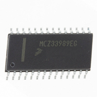
MCZ33989EG Freescale Semiconductor, MCZ33989EG Datasheet - Page 43

MCZ33989EG
Manufacturer Part Number
MCZ33989EG
Description
IC SYSTEM BASIS CHIP CAN 28-SOIC
Manufacturer
Freescale Semiconductor
Datasheet
1.MC33989DWR2.pdf
(66 pages)
Specifications of MCZ33989EG
Applications
*
Interface
*
Voltage - Supply
*
Package / Case
28-SOIC (7.5mm Width)
Mounting Type
Surface Mount
Lead Free Status / RoHS Status
Lead free / RoHS Compliant
Available stocks
Company
Part Number
Manufacturer
Quantity
Price
Part Number:
MCZ33989EG
Manufacturer:
FREESCALE
Quantity:
20 000
Company:
Part Number:
MCZ33989EGR2
Manufacturer:
EXAR
Quantity:
6 247
WAKE-UP TIMING: STOP MODE
from stop mode, and the sequence of the signals at the SBC
Analog Integrated Circuit Device Data
Freescale Semiconductor
• T1(third valid CAN dominant pulse to V
• T2 and T3 identical to page
• The total time is 6.58 ms in this example.
• T1: Is dependent on the selected cyclic sense timing in
• 10 µs before the end of cyclic sense on time. If the LX
• point, the wake-up will be detected at the next HS1
• T2: It is the same time as LX to VDD1 turn on: typ
• T3 & T4: same as page
• The total time is 11.5 ms (for a cyclic sense total time of
The following paragraphs describe the wake-up events
80 µs.
the TIM2 register (5 ms to 400 ms). LX is sampled
correct wake-up level happens just after the sample
activation and a complete period is lost.
100 µs
5 ms) in this example.
LX
VDD1
RESET
HS1
RST
RESET
CAN
VDD1
RST
39
39
tCAN
above
t1
DD1
turn on): typ
Figure 27. CAN Wake-Up
t1
t2
Figure 28.
t3
LX with Cyclic Sense
associated with the cyclic sense function.
level. The wake-up time described is the time from the wake-
up event to the SBC INT pin. The wake-up time is the sum of
several timings: wake-up signal detection, the INT pulse, and
a minimum delay between INT and SBC ready to operate. At
the end of the wake-up time, the SBC is ready to operate,
however the MCU might have already been in a restart
operation.
LX Wake-Up
awakened by an LX positive edge
t2
The case below is a description of the wake-up by LX input
Below is the case where the SBC is in stop mode and is
• T1(L0 high level to INT pulse): typ 100 µs.
• The total time is 133 µs in this case.
t4
SUPPLEMENTAL APPLICATION NOTES
t3
TYPICAL APPLICATIONS
33989
43


