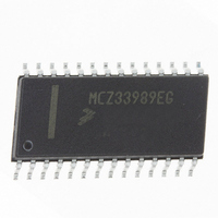
MCZ33989EG Freescale Semiconductor, MCZ33989EG Datasheet - Page 42

MCZ33989EG
Manufacturer Part Number
MCZ33989EG
Description
IC SYSTEM BASIS CHIP CAN 28-SOIC
Manufacturer
Freescale Semiconductor
Datasheet
1.MC33989DWR2.pdf
(66 pages)
Specifications of MCZ33989EG
Applications
*
Interface
*
Voltage - Supply
*
Package / Case
28-SOIC (7.5mm Width)
Mounting Type
Surface Mount
Lead Free Status / RoHS Status
Lead free / RoHS Compliant
Available stocks
Company
Part Number
Manufacturer
Quantity
Price
Part Number:
MCZ33989EG
Manufacturer:
FREESCALE
Quantity:
20 000
Company:
Part Number:
MCZ33989EGR2
Manufacturer:
EXAR
Quantity:
6 247
Power Up and V
Default Low Power Mode Selected
figure. If V
(typ 4.6 V) for instance by an over current or short circuit (ex
short to 4 V), and if the low power mode previously selected
was sleep mode and if the BATFAIL flag has been cleared,
WAKE-UP TIMINGS — SLEEP MODE
sleep mode, and the sequence of the signals at the SBC
level. The wake-up time described is the time from the wake-
up event to the SBC reset pin release. The wake-up time is
the sum of several timings: wake-up signal detection, V
regulator start-up and decoupling capacitor charge, and reset
42
33989
TYPICAL APPLICATIONS
SUPPLEMENTAL APPLICATION NOTES
SPI (CS)
VDD1
WD
RST
INT
The first part of the graph is the same as the previous
The paragraphs below describe the wake-up events from
• T1 (LX high level to V
• T2: V
the load connected to V
the capacitor charging time with the regulator output
current limitation: T2 = (C x U)/I. With C = 100 mF,
I
DD1
VDD1
= 200 mA min., U = 5 V so T2 = 2.5 ms).
DD1
RST
DD1
LX
S B C in
R E S E T
m o d e
Figure 25. Power up and V
is pulled below the V
rising time is dependent on the capacitor and
DD1
350 ms
Going Low with Sleep Mode as
Reset every 350 ms
S B C in N o rm a l re q u e s t
m o d e
DD1
t1
DD1
turn on): typ 100 µs.
. It can be approximated by
DD1
under voltage reset
DD1
Going Low with Sleep Mode as Default Low Power Mode Selected
t2
DD1
Figure 26.
S B C in N o rm a l
m o d e
Write Watchdog
each X ms
the SBC enters reset mode for a time period of 100 ms. The
pin WD stays high, but the high level (V
level.The reset and interrupt pins are low. After the 100 ms,
the SBC goes into sleep mode. V
following figure is an example where V
and after 100 ms the SBC enters sleep mode.
time. At the end of the reset time, the reset pin goes from low
to high and the MCU is ready to start software operations.
LX Wakes up SBC from Sleep Mode
awaked by LX positive edge.
CAN Wake-Up
Refer to page
and the TCAN analysis.
t3
Below is the case where the SBC is in sleep mode and is
• T3 (VDD1>RST-TH (4.6 V by default) to reset high):
• The total time is 6.6 ms in this example.
The following case describes the signal for CAN wake up.
parameter Rest dur: 4 ms max.
S B C in R e s e t
m o d e
(B A T F A IL fla g
m u s t b e c le a re d )
49
for more details on CAN wake up signals
1 0 0 m s
S B C in S le e p m o d e
Analog Integrated Circuit Device Data
Watchdog period
No problem on
DD1
Freescale Semiconductor
and V2 are off (The
DD1
OH
) follows the V
is shorted to 4 V,
DD1


