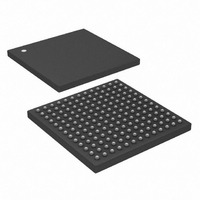
DS33Z11+ Maxim Integrated Products, DS33Z11+ Datasheet - Page 30

DS33Z11+
Manufacturer Part Number
DS33Z11+
Description
IC MAPPER ETHERNET 169-CSBGA
Manufacturer
Maxim Integrated Products
Datasheet
1.DS33Z11.pdf
(172 pages)
Specifications of DS33Z11+
Applications
Data Transport
Interface
SPI/Parallel
Voltage - Supply
1.8V, 3.3V
Package / Case
169-CSBGA
Mounting Type
Surface Mount
Lead Free Status / RoHS Status
Lead free / RoHS Compliant
- Current page: 30 of 172
- Download datasheet (2Mb)
8.1.1 Read-Write/Data Strobe Modes
The processor interface can operate in either read-write strobe mode or data strobe mode. When MODEC[1:0] =
00 and HWMODE pin = 0 the read-write strobe mode is enabled and a negative pulse on RD performs a read
cycle, and a negative pulse on WR performs a write cycle. When MODEC[1:0] pins = 01 and HWMODE pin = 0
the data strobe mode is enabled and a negative pulse on DS when RW is high performs a read cycle, and a
negative pulse on DS when RW is low performs a write cycle. The read-write strobe mode is commonly called the
“Intel” mode, and the data strobe mode is commonly called the “Motorola” mode.
8.1.2
The latched status registers will clear on a read access. It is important to note that in a multi-task software
environment, the user should handle all status conditions of each register at the same time to avoid inadvertently
clearing status conditions. The latched status register bits are carefully designed so that an event occurrence
cannot collide with a user read access.
8.1.3
The interrupt (INT) pin is configurable to drive high or float when not active. The INTM bit controls the pin
configuration, when it is set the INT pin will drive high when not active. After reset, the INT pin is in high-
impedance mode until an interrupt source is active and enabled to drive the interrupt pin.
8.2 SPI Serial EEPROM Interface
The SPI interface is a 4 signal serial interface that allows connection to a serial EEPROM for initialization
information. The DS33Z11 will act as an SPI Master when configured with MODEC[1:0] to read from an external
Serial EEPROM. The reading sequence is commenced upon initial reset or rising edge of the RST input pin. The
CKPHA pin controls the sampling and update edges of the MISO and MOSI signals. The MISO data can be
sampled on rising or falling edge of SPICK. The MOSI (Master Out Slave In) can be selectively output on the
rising or falling edge of SPICK. The SPICK is generated by the DS33Z11 at a frequency of 8.33 MHz. This
frequency is derived from an external SYSCLKI (100 MHz). The instruction to initiate a read is 0000x011; this is
followed by the address location 0. The SPI_CS is low till the data addressed
The DS33Z11 will provide the starting address (0000000) and the data is sequentially latched till the last data is
read and latched. The MAC specific registers, which are addressed indirectly, are written at the end of the normal
control registers. More details of the programming sequence an functional timing information can be found in
Section 10.3. The indirect registers related to the MAC are programmed using a special command format as
shown in
Clear on Read
Interrupt and Pin Modes
Table
10-2.
30 of 172
(Table
10-1) is read and latched.
Related parts for DS33Z11+
Image
Part Number
Description
Manufacturer
Datasheet
Request
R

Part Number:
Description:
MAX7528KCWPMaxim Integrated Products [CMOS Dual 8-Bit Buffered Multiplying DACs]
Manufacturer:
Maxim Integrated Products
Datasheet:

Part Number:
Description:
Single +5V, fully integrated, 1.25Gbps laser diode driver.
Manufacturer:
Maxim Integrated Products
Datasheet:

Part Number:
Description:
Single +5V, fully integrated, 155Mbps laser diode driver.
Manufacturer:
Maxim Integrated Products
Datasheet:

Part Number:
Description:
VRD11/VRD10, K8 Rev F 2/3/4-Phase PWM Controllers with Integrated Dual MOSFET Drivers
Manufacturer:
Maxim Integrated Products
Datasheet:

Part Number:
Description:
Highly Integrated Level 2 SMBus Battery Chargers
Manufacturer:
Maxim Integrated Products
Datasheet:

Part Number:
Description:
Current Monitor and Accumulator with Integrated Sense Resistor; ; Temperature Range: -40°C to +85°C
Manufacturer:
Maxim Integrated Products

Part Number:
Description:
TSSOP 14/A�/RS-485 Transceivers with Integrated 100O/120O Termination Resis
Manufacturer:
Maxim Integrated Products

Part Number:
Description:
TSSOP 14/A�/RS-485 Transceivers with Integrated 100O/120O Termination Resis
Manufacturer:
Maxim Integrated Products

Part Number:
Description:
QFN 16/A�/AC-DC and DC-DC Peak-Current-Mode Converters with Integrated Step
Manufacturer:
Maxim Integrated Products

Part Number:
Description:
TDFN/A/65V, 1A, 600KHZ, SYNCHRONOUS STEP-DOWN REGULATOR WITH INTEGRATED SWI
Manufacturer:
Maxim Integrated Products

Part Number:
Description:
Integrated Temperature Controller f
Manufacturer:
Maxim Integrated Products

Part Number:
Description:
SOT23-6/I�/45MHz to 650MHz, Integrated IF VCOs with Differential Output
Manufacturer:
Maxim Integrated Products

Part Number:
Description:
SOT23-6/I�/45MHz to 650MHz, Integrated IF VCOs with Differential Output
Manufacturer:
Maxim Integrated Products

Part Number:
Description:
EVALUATION KIT/2.4GHZ TO 2.5GHZ 802.11G/B RF TRANSCEIVER WITH INTEGRATED PA
Manufacturer:
Maxim Integrated Products

Part Number:
Description:
QFN/E/DUAL PCIE/SATA HIGH SPEED SWITCH WITH INTEGRATED BIAS RESISTOR
Manufacturer:
Maxim Integrated Products
Datasheet:


