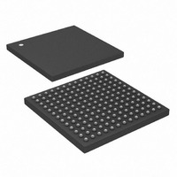
DS33Z11+ Maxim Integrated Products, DS33Z11+ Datasheet - Page 22

DS33Z11+
Manufacturer Part Number
DS33Z11+
Description
IC MAPPER ETHERNET 169-CSBGA
Manufacturer
Maxim Integrated Products
Datasheet
1.DS33Z11.pdf
(172 pages)
Specifications of DS33Z11+
Applications
Data Transport
Interface
SPI/Parallel
Voltage - Supply
1.8V, 3.3V
Package / Case
169-CSBGA
Mounting Type
Surface Mount
Lead Free Status / RoHS Status
Lead free / RoHS Compliant
- Current page: 22 of 172
- Download datasheet (2Mb)
CKPHA
WR/RW
SPI_CS
NAME
RD/DS
RST
INT
CS
D6
D7
DS33Z11
CSBGA
PIN #
(169)
C5
C6
B8
C1
E1
E2
D8
F6
F3
DS33ZH1
BGA(100)
PIN #
C1
B5
—
—
—
—
—
—
—
1
TYPE
IOZ
IOZ
OZ
O
I
I
I
I
I
22 of 172
Data Bit 6: Bidirectional data bit 6 of the microprocessor
interface. Not driven when CS = 1 or RST = 0.
Data Bit 7: Bidirectional data bit 7 of the microprocessor
interface. Most Significant Bit. CS = 1 or RST = 0.
Active-Low SPI Chip Select: Provides the chip select to
the external EEPROM, when the SPI port is in master
mode.
SPI Clock Phase: MISO is sampled on the falling edge
when CKPHA is set high, and on the rising edge when set
low.
MOSI is updated on the rising edge when CKPHA is set
high, and on the falling edge when set low.
Active-Low Chip Select: This pin must be taken low for
read/write operations. When CS is high, the RD/DS and
WR signals are ignored.
Active-Low Read-Data Strobe (Intel Mode): The
DS33Z11 drives the data bus (D0-D7) with the contents of
the addressed register while RD and CS are both low.
Active-Low Data Strobe (Motorola Mode): Used to latch
data through the microprocessor interface. DS must be
low during read and write operations.
Active-Low Write (Intel Mode): The DS33Z11 captures
the contents of the data bus (D0-D7) on the rising edge of
WR and writes them to the addressed register location.
CS must be held low during write operations.
Read Write (Motorola Mode): Used to indicate read or
write operation. RW must be set high for a register read
cycle and low for a register write cycle.
Active-Low Interrupt Output: Outputs a logic zero when
an unmasked interrupt event is detected. INT is
deasserted when all interrupts have been acknowledged
and serviced. Inactive state is programmable in register
GL.CR1.
Active-Low Reset: An active low signal on this pin resets
the internal registers and logic. This pin should remain low
until power, SYSCLKI, RX_CLK, and TX_CLK are stable,
then set high for normal operation. In DCE and RMII
modes, the REF_CLK input must also have a stable clock
input before setting RST high for normal operation. This
input requires a clean edge with a rise time of 25ns or less
to properly reset the device.
FUNCTION
Related parts for DS33Z11+
Image
Part Number
Description
Manufacturer
Datasheet
Request
R

Part Number:
Description:
MAX7528KCWPMaxim Integrated Products [CMOS Dual 8-Bit Buffered Multiplying DACs]
Manufacturer:
Maxim Integrated Products
Datasheet:

Part Number:
Description:
Single +5V, fully integrated, 1.25Gbps laser diode driver.
Manufacturer:
Maxim Integrated Products
Datasheet:

Part Number:
Description:
Single +5V, fully integrated, 155Mbps laser diode driver.
Manufacturer:
Maxim Integrated Products
Datasheet:

Part Number:
Description:
VRD11/VRD10, K8 Rev F 2/3/4-Phase PWM Controllers with Integrated Dual MOSFET Drivers
Manufacturer:
Maxim Integrated Products
Datasheet:

Part Number:
Description:
Highly Integrated Level 2 SMBus Battery Chargers
Manufacturer:
Maxim Integrated Products
Datasheet:

Part Number:
Description:
Current Monitor and Accumulator with Integrated Sense Resistor; ; Temperature Range: -40°C to +85°C
Manufacturer:
Maxim Integrated Products

Part Number:
Description:
TSSOP 14/A�/RS-485 Transceivers with Integrated 100O/120O Termination Resis
Manufacturer:
Maxim Integrated Products

Part Number:
Description:
TSSOP 14/A�/RS-485 Transceivers with Integrated 100O/120O Termination Resis
Manufacturer:
Maxim Integrated Products

Part Number:
Description:
QFN 16/A�/AC-DC and DC-DC Peak-Current-Mode Converters with Integrated Step
Manufacturer:
Maxim Integrated Products

Part Number:
Description:
TDFN/A/65V, 1A, 600KHZ, SYNCHRONOUS STEP-DOWN REGULATOR WITH INTEGRATED SWI
Manufacturer:
Maxim Integrated Products

Part Number:
Description:
Integrated Temperature Controller f
Manufacturer:
Maxim Integrated Products

Part Number:
Description:
SOT23-6/I�/45MHz to 650MHz, Integrated IF VCOs with Differential Output
Manufacturer:
Maxim Integrated Products

Part Number:
Description:
SOT23-6/I�/45MHz to 650MHz, Integrated IF VCOs with Differential Output
Manufacturer:
Maxim Integrated Products

Part Number:
Description:
EVALUATION KIT/2.4GHZ TO 2.5GHZ 802.11G/B RF TRANSCEIVER WITH INTEGRATED PA
Manufacturer:
Maxim Integrated Products

Part Number:
Description:
QFN/E/DUAL PCIE/SATA HIGH SPEED SWITCH WITH INTEGRATED BIAS RESISTOR
Manufacturer:
Maxim Integrated Products
Datasheet:


