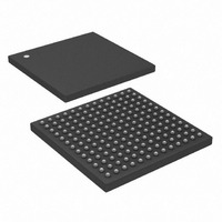
DS33Z11+ Maxim Integrated Products, DS33Z11+ Datasheet - Page 17

DS33Z11+
Manufacturer Part Number
DS33Z11+
Description
IC MAPPER ETHERNET 169-CSBGA
Manufacturer
Maxim Integrated Products
Datasheet
1.DS33Z11.pdf
(172 pages)
Specifications of DS33Z11+
Applications
Data Transport
Interface
SPI/Parallel
Voltage - Supply
1.8V, 3.3V
Package / Case
169-CSBGA
Mounting Type
Surface Mount
Lead Free Status / RoHS Status
Lead free / RoHS Compliant
- Current page: 17 of 172
- Download datasheet (2Mb)
7
7.1 Pin Functional Description
Note that all digital pins are IO pins in JTAG mode. This feature increases the effectiveness of board level ATPG
patterns. JTAG pins are not available on the Hardware mode/SPI-only DS33ZH11 (10mm CSBGA)
Note: I = Input; O = Output; Ipu = Input, with pullup; Oz = Output, with tri-state; IO = Bidirectional pin; IOz = Bidirectional pin, with tri-state
Table 7-1 Detailed Pin Descriptions
TBSYNC
NAME
TDEN/
RCLKI
PIN DESCRIPTIONS
TCLKI
RSER
TSER
DS33Z11
CSBGA
PIN #
(169)
G2
H1
F1
F2
F5
DS33ZH1
BGA(100)
PIN #
B1
A2
B2
B3
—
1
SERIAL INTERFACE IO PINS
TYPE
IO
O
I
I
I
17 of 172
Serial Interface Transmit Clock Input: The clock
reference for TSER, which is output on the rising edge of
the clock. TCLKI supports gapped clocking, up to a
maximum frequency of 52 MHz.
Transmit Serial Data Output: Output on the rising edge
of TCLKI. Selective clock periods can be skipped for
output of TSER dependent on the TDEN settings or
gapped clock input (TCLKI). The maximum data rate is 52
Mbps.
Transmit Data Enable (Input): The transmit data enable
is programmable to selectively block/enable the transmit
data. The TDEN signal must occur one clock edge prior to
the affected data bit. The active polarity of TDEN is
programmable in register LI.TSLCR. It is recommended
for both T1/E1 and T3/E3 applications that use gapped
clocks. The TDEN signal is provided for interfacing to
framers that do not have a gapped clock facility.
Transmit Byte Sync (Output): This output can be used
by an external Serial to Parallel to convert TSER stream to
byte wide data. This output indicates the last bit of the
byte data sent serially on TSER. This signal is only active
in the X.86 Mode.
Note that while in Hardware mode with HDLC (non X.86)
operation, this pin must be tied high.
Serial Interface Receive Clock Input: Reference clock
for receive serial data on RSER. Gapped clocking is
supported, up to the maximum RCLKI frequency of 52
MHz.
Receive Serial Data Input: Receive Serial data arrives on
the rising edge of the clock.
FUNCTION
Related parts for DS33Z11+
Image
Part Number
Description
Manufacturer
Datasheet
Request
R

Part Number:
Description:
MAX7528KCWPMaxim Integrated Products [CMOS Dual 8-Bit Buffered Multiplying DACs]
Manufacturer:
Maxim Integrated Products
Datasheet:

Part Number:
Description:
Single +5V, fully integrated, 1.25Gbps laser diode driver.
Manufacturer:
Maxim Integrated Products
Datasheet:

Part Number:
Description:
Single +5V, fully integrated, 155Mbps laser diode driver.
Manufacturer:
Maxim Integrated Products
Datasheet:

Part Number:
Description:
VRD11/VRD10, K8 Rev F 2/3/4-Phase PWM Controllers with Integrated Dual MOSFET Drivers
Manufacturer:
Maxim Integrated Products
Datasheet:

Part Number:
Description:
Highly Integrated Level 2 SMBus Battery Chargers
Manufacturer:
Maxim Integrated Products
Datasheet:

Part Number:
Description:
Current Monitor and Accumulator with Integrated Sense Resistor; ; Temperature Range: -40°C to +85°C
Manufacturer:
Maxim Integrated Products

Part Number:
Description:
TSSOP 14/A�/RS-485 Transceivers with Integrated 100O/120O Termination Resis
Manufacturer:
Maxim Integrated Products

Part Number:
Description:
TSSOP 14/A�/RS-485 Transceivers with Integrated 100O/120O Termination Resis
Manufacturer:
Maxim Integrated Products

Part Number:
Description:
QFN 16/A�/AC-DC and DC-DC Peak-Current-Mode Converters with Integrated Step
Manufacturer:
Maxim Integrated Products

Part Number:
Description:
TDFN/A/65V, 1A, 600KHZ, SYNCHRONOUS STEP-DOWN REGULATOR WITH INTEGRATED SWI
Manufacturer:
Maxim Integrated Products

Part Number:
Description:
Integrated Temperature Controller f
Manufacturer:
Maxim Integrated Products

Part Number:
Description:
SOT23-6/I�/45MHz to 650MHz, Integrated IF VCOs with Differential Output
Manufacturer:
Maxim Integrated Products

Part Number:
Description:
SOT23-6/I�/45MHz to 650MHz, Integrated IF VCOs with Differential Output
Manufacturer:
Maxim Integrated Products

Part Number:
Description:
EVALUATION KIT/2.4GHZ TO 2.5GHZ 802.11G/B RF TRANSCEIVER WITH INTEGRATED PA
Manufacturer:
Maxim Integrated Products

Part Number:
Description:
QFN/E/DUAL PCIE/SATA HIGH SPEED SWITCH WITH INTEGRATED BIAS RESISTOR
Manufacturer:
Maxim Integrated Products
Datasheet:


