PI7C9X20404GPBNBE Pericom Semiconductor, PI7C9X20404GPBNBE Datasheet
PI7C9X20404GPBNBE
Specifications of PI7C9X20404GPBNBE
Available stocks


Related parts for PI7C9X20404GPBNBE

PI7C9X20404GPBNBE Summary of contents
Page 1
PI7C9X20404GP PCI EXPRESS PACKET SWITCH DATASHEET REVISION 1.6 June 2009 ST 3545 North 1 Street, San Jose, CA 95134 Telephone: 1-877-PERICOM, (1-877-737-4266) FAX: 408-435-1100 Internet: http://www.pericom.com ...
Page 2
... A critical component is any component of a life support device or system whose failure to perform can be reasonably expected to cause the failure of the life support device or system affect its safety or effectiveness. Pericom Semiconductor Corporation reserves the right to make changes to its products or specifications at any time, without notice, in order to improve design or performance and to supply the best possible product ...
Page 3
... Updated 5.1 Physical Layer Circuit and Chapter 5.6 Queue Updated Disclaimer and Footer Updated Chapter 14 Ordering Information Fixed Chapter 6.1.4 Mapping EEPROM format 1/11/08 1.0 Modified Chapter 3.4 MISCELLANEOUS SIGNALS June 2009 – Revision 1.6 Pericom Semiconductor 4Port-4Lane PCI Express Switch Page PI7C9X20404GP TM GreenPacket Family Datasheet ...
Page 4
... Updated Chapter 3.3 Hot Plug Signals (PWR_IND, ATT_IND) Updated Chapter 3.4 Miscellaneous Signals (PWR_SAV pin removed, EEPD) Updated Chapter 3.5 JTAG Boundary Scan Signals (TMS, TDI, TRST_L) June 2009 – Revision 1.6 Pericom Semiconductor 4Port-4Lane PCI Express Switch Page PI7C9X20404GP TM GreenPacket ...
Page 5
... DEVICE ID REGISTER – OFFSET 00h.............................................................................................32 7.2.3 COMMAND REGISTER – OFFSET 04h............................................................................................32 7.2.4 PRIMARY STATUS REGISTER – OFFSET 04h.................................................................................33 7.2.5 REVISION ID REGISTER – OFFSET 08h .........................................................................................33 June 2009 – Revision 1.6 Pericom Semiconductor 4Port-4Lane PCI Express Switch Page PI7C9X20404GP TM GreenPacket Family Datasheet ...
Page 6
... NEXT ITEM POINTER REGISTER – OFFSET B8h ..........................................................................46 7.2.56 SUBSYSTEM VENDOR ID REGISTER – OFFSET BCh....................................................................46 7.2.57 SUBSYSTEM ID REGISTER – OFFSET BCh ....................................................................................46 7.2.58 GPIO CONTROL REGISTER – OFFSET D8h (Upstream Port Only)...............................................46 June 2009 – Revision 1.6 Pericom Semiconductor 4Port-4Lane PCI Express Switch Page PI7C9X20404GP TM GreenPacket Family Datasheet ...
Page 7
... POWER BUDGETING DATA REGISTER – OFFSET 214h ..........................................................66 7.2.104 POWER BUDGET CAPABILITY REGISTER – OFFSET 218h .....................................................67 8 CLOCK SCHEME .............................................................................................................................................68 9 HOT PLUG OPERATION ................................................................................................................................69 10 IEEE 1149.1 COMPATIBLE JTAG CONTROLLER....................................................................................70 10.1 INSTRUCTION REGISTER ......................................................................................................................70 June 2009 – Revision 1.6 Pericom Semiconductor 4Port-4Lane PCI Express Switch Page PI7C9X20404GP TM GreenPacket Family Datasheet ...
Page 8
... JTAG BOUNDARY SCAN REGISTER ORDER......................................................................................71 11 POWER MANAGEMENT ................................................................................................................................73 12 ELECTRICAL AND TIMING SPECIFICATIONS .......................................................................................74 12.1 ABSOLUTE MAXIMUM RATINGS ........................................................................................................74 12.2 DC SPECIFICATIONS ..............................................................................................................................74 12.3 AC SPECIFICATIONS ..............................................................................................................................75 13 PACKAGE INFORMATION............................................................................................................................77 14 ORDERING INFORMATION..........................................................................................................................79 June 2009 – Revision 1.6 Pericom Semiconductor 4Port-4Lane PCI Express Switch Page PI7C9X20404GP TM GreenPacket Family Datasheet ...
Page 9
... ABLE BOUNDARY SCAR REGISTER DEFINITION T 12-1 A ABLE BSOLUTE MAXIMUM RATINGS T 12-2 DC ABLE ELECTRICAL CHARACTERISTICS T 12 ABLE RANSMITTER HARACTERISTICS T 12 ABLE ECEIVER HARACTERISTICS June 2009 – Revision 1.6 Pericom Semiconductor I PI7C9X20404GP............................................................29 MPLEMENTATION ON ........................................................................................................................77 ................................................................................................................. )............................................................................................16 ALUES NOM N C .............................................................................16 OMINAL URRENT DEQ [3:0]................................................................................................... ..........................................................................................20 RDERING ULES .................................................................................................... ...
Page 10
... Programmable driver current and de-emphasis level at each individual port Low Power Dissipation at 0.8W typical in L0 normal mode Industrial Temperature Range -40 148-pin LFBGA 12mm x 12mm package, 0.8 mm Ball Pitch June 2009 – Revision 1.6 Pericom Semiconductor and L3 link power states Ready and D3 device power states ...
Page 11
... VC1 queues can be reassigned to VC0 and enable each of the ingress ports to handle more data traffic bursts. This virtual channel resource relocation feature enhances the performance of the PCIe Switch further. June 2009 – Revision 1.6 Pericom Semiconductor 4Port-4Lane PCI Express Switch Page PI7C9X20404GP ...
Page 12
... B1 SLOT_IMP [3:1] B4, C4, E3 HOTPLUG [3:1] A5, B5, C5 SLOTCLK F3 June 2009 – Revision 1.6 Pericom Semiconductor 4Port-4Lane PCI Express Switch TYPE DESCRIPTION I Reference Clock Input Pairs: Connect to external 100MHz differential clock. The input clock signals must be delivered to the clock buffer cell through an AC-coupled interface so that only the AC information of the clock is received, converted, and buffered ...
Page 13
... NC A10, A12, A14, B10, B12, B14, H3, L1, M2, M3, M4, N3 June 2009 – Revision 1.6 Pericom Semiconductor 4Port-4Lane PCI Express Switch TYPE DESCRIPTION O Power Indicator: Indicates the power status for each slot at downstream port. PWR_IND [x] is correspondent to Port x, where x=1,2,3. They are active-high signals. The pins have internal pull- down ...
Page 14
... F13, F14, G8, G13, H8, H13, J8, M13, M14, N13, P1, P3, P9 June 2009 – Revision 1.6 Pericom Semiconductor 4Port-4Lane PCI Express Switch TYPE DESCRIPTION I Test Clock: Used to clock state information and data into and out of the chip during boundary scan. When JTAG boundary scan function is not implemented, this pin should be left open (NC) ...
Page 15
... B11 TEST6 B12 NC B13 VSS B14 NC C1 GPIO[2] C2 DWNRST_L[1] C3 TEST2 C4 SLOT_IMP[2] C5 HOTPLUG[1] C6 TEST3 C7 VDDC C8 VSS C9 VDDA June 2009 – Revision 1.6 Pericom Semiconductor PIN NAME PIN C10 VSS H1 C11 VSS H2 C12 VDDR H3 C13 VSS H6 C14 VSS H7 D1 GPIO[ RESET_L H9 D3 VDDCAUX ...
Page 16
... Table 5-2 Ratio of Actual Current and Nominal Current DTX [3:0] ACTUAL CURRENT / NOMINAL CURRENT 0000 0001 0010 0011 0100 0101 0110 1 Multiple lanes could share the PLL. June 2009 – Revision 1.6 Pericom Semiconductor NOMINAL DRIVER CURENT Reserved 1.00 1.05 1.10 1 ...
Page 17
... ISI related jitter. The following table shows a simple guideline for selecting the appropriate value to adapt with different lengths or connector numbers in various applications. Table 5-4 Rx Equalizer Settings (RXEQCTL) RXEQCTL [1] RXEQCTL [ June 2009 – Revision 1.6 Pericom Semiconductor 1.35 0.60 0.65 0.70 0.75 0.80 0.85 0.90 0.95 –I ...
Page 18
... If the incoming packet can not be forwarded to any other port due to a miss to hit the defined address range or targeted ID, this is considered as Unsupported Request (UR) packet, which is similar to a master abort event in PCI protocol. June 2009 – Revision 1.6 Pericom Semiconductor 4Port-4Lane PCI Express Switch Page PI7C9X20404GP ...
Page 19
... CPLH queue provides TLP header space for completion packets. Each header space takes twelve bytes to accommodate a 3-DW header. Please note that there is no 4-DW completion headers. There are two CPLH queues for VC0 and VC1 respectively. June 2009 – Revision 1.6 Pericom Semiconductor 4Port-4Lane PCI Express Switch Page PI7C9X20404GP ...
Page 20
... Completions. Otherwise, deadlocks may occur when some older Bridges that do not support delayed transactions are mixed with PCIe Switch in the same system. A fairness algorithm is used to arbitrate between the Posted Write queue and the Non-posted transaction queue. June 2009 – Revision 1.6 Pericom Semiconductor Read Non-posted Write Request ...
Page 21
... TLP generated from VC arbiter, respond with the completion packet when the local resource (i.e. configuration register) is accessed and regenerate the message that terminated at receiver acts as an upstream port. June 2009 – Revision 1.6 Pericom Semiconductor 4Port-4Lane PCI Express Switch Page PI7C9X20404GP ...
Page 22
... Extended VC Count / Link Capability / Switch Mode Operation / Interrupt pin for Port Max_Payload_Size Support / ASPM Support / Role_Base Error Reporting / RefClk ppm PM Data for Port 0 PM Data for Port 1 PM Data for Port 2 PM Data for Port 3 June 2009 – Revision 1.6 Pericom Semiconductor 7 – 0 Vendor ID Device ID Subsystem Vender ID Subsystem ID Difference ...
Page 23
... Acknowledge Latency Timer for Port 0 Acknowledge Latency Timer for Port 1 Acknowledge Latency Timer for Port 2 Acknowledge Latency Timer for Port 3 June 2009 – Revision 1.6 Pericom Semiconductor 7 – 0 Reserved Slot Clock / LPVC Count / Port Num, Port 0 Slot Implemented / Slot Clock / LPVC Count ...
Page 24
... B0h : Bit [14] B0h(port 0~3) B0h : Bit [15] B4h(port 0~3) B4h : Bit [15] B0h(port 0~3) B0h : Bit [13] A8h(Port 0~3) June 2009 – Revision 1.6 Pericom Semiconductor 7 – 0 PHY Parameter for Port 2 PHY Parameter for Port 3 Reserved Reserved Reserved Reserved PM Control Para/Rx Polarity for Port 0 ...
Page 25
... Bit [4] ECh (Port 0) ECh: Bit [25:24] June 2009 – Revision 1.6 Pericom Semiconductor 4Port-4Lane PCI Express Switch DESCRIPTION Bit [9:8]: It represents RefClk ppm difference between the two ends in one link; 00: 0 ppm, 01: 100 ppm, 10: 200 ppm, 11: 300 ...
Page 26
... F4h (Port 1) F4h: Bit [15:0] 34h F4h (Port 2) F4h: Bit [15:0] June 2009 – Revision 1.6 Pericom Semiconductor 4Port-4Lane PCI Express Switch DESCRIPTION VC0 TC/VC Map for Port 0 Bit [15:9]: When set, it indicates the corresponding TC is mapped into VC0 PCIe Capability Slot Implemented for Port 1 ...
Page 27
... B0h (Port 3) B0h – Bit [31:16] 90h B4h (Port 0) B4h: Bit [31:16] June 2009 – Revision 1.6 Pericom Semiconductor 4Port-4Lane PCI Express Switch DESCRIPTION Slot Capability 0 of Port 3 Bit [15:0]: Mapping to the low word of slot capability register Slot Capability 1 of Port 1 ...
Page 28
... B4h (Port 2) B4h : Bit [14] A6h B4h (Port 3) B4h: Bit [13:8] B4h (Port 3) B4h : Bit [14] June 2009 – Revision 1.6 Pericom Semiconductor 4Port-4Lane PCI Express Switch DESCRIPTION PHY Parameter for Port 1 Bit [31:16]: PHY Parameter PHY Parameter for Port 2 Bit [31:16]: PHY Parameter PHY Parameter for Port 3 ...
Page 29
... Table 6-1 SMBus Address Pin Configuration BIT SMBus Address 0 GPIO[5] 1 GPIO[6] 2 GPIO[ June 2009 – Revision 1.6 Pericom Semiconductor 4Port-4Lane PCI Express Switch Processor Other SMBus (SMBus Master) Devices Page PI7C9X20404GP TM GreenPacket Family Datasheet ...
Page 30
... Message Control Reserved VPD Register Length in Bytes (14h) ACK Latency Timer Reserved SSID June 2009 – Revision 1.6 Pericom Semiconductor DEFINITION Hardware Initialization Read Only Read / Write Read / Write 1 to Clear Sticky - Read Only / Write 1 to Clear Sticky - Read / Write Sticky – Read Only 23 – ...
Page 31
... Port VC Status Register Port Arbitration Table Offset=4 VC Resource Status Register (0) Port Arbitration Table Offset=6 VC Resource Status Register (1) Next Capability Offset=000h June 2009 – Revision 1.6 Pericom Semiconductor 23 – EEPROM Address Next Item Pointer=00 Device Capabilities Device Control Link Capabilities Link Control ...
Page 32
... Wait Cycle Control 8 SERR# enable Fast Back-to-Back 9 Enable 10 Interrupt Disable June 2009 – Revision 1.6 Pericom Semiconductor 4Port-4Lane PCI Express Switch TYPE DESCRIPTION RO Identifies Pericom as the vendor of this device. The default value may be changed by SMBus or auto-loading from EEPROM. Reset to 12D8h. TYPE ...
Page 33
... CLASS CODE REGISTER – OFFSET 08h BIT FUNCTION 15:8 Programming Interface 23:16 Sub-Class Code 31:24 Base Class Code June 2009 – Revision 1.6 Pericom Semiconductor 4Port-4Lane PCI Express Switch TYPE DESCRIPTION RO Reset to 0b. TYPE DESCRIPTION RO Reset to 000b. Indicates that an INTx Interrupt Message is pending internally to the device. ...
Page 34
... BIT FUNCTION Subordinate Bus 23:16 Number June 2009 – Revision 1.6 Pericom Semiconductor 4Port-4Lane PCI Express Switch TYPE DESCRIPTION The cache line size register is set by the system firmware and the operating system cache line size. This field is implemented by PCI Express devices as a ...
Page 35
... Error 26:25 DEVSEL_L timing Signaled Target 27 Abort Received Target 28 Abort June 2009 – Revision 1.6 Pericom Semiconductor 4Port-4Lane PCI Express Switch TYPE DESCRIPTION Does not apply to PCI Express. Must be hardwired to 00h. RO TYPE DESCRIPTION RO Read as 01h to indicate 32-bit I/O addressing. Defines the bottom address of the I/O address range for the Bridge to determine when to forward I/O transactions from one interface to the other ...
Page 36
... PREFETCHABLE MEMORY LIMIT ADDRESS REGISTER – OFFSET 24h BIT FUNCTION 19:16 64-bit addressing June 2009 – Revision 1.6 Pericom Semiconductor 4Port-4Lane PCI Express Switch TYPE DESCRIPTION Set to 1 (by a requestor) whenever receiving a Completion with Unsupported Request Completion Status in secondary side. RO Reset to 0b ...
Page 37
... CAPABILITY POINTER REGISTER – OFFSET 34h BIT FUNCTION 7:0 Capability Pointer June 2009 – Revision 1.6 Pericom Semiconductor 4Port-4Lane PCI Express Switch TYPE DESCRIPTION Defines the top address of an address range for the Bridge to determine when to forward memory read and write transactions from one interface to the other ...
Page 38
... ISA Enable 19 VGA Enable 20 VGA 16-bit decode 21 Master Abort Mode 22 Secondary Bus Reset June 2009 – Revision 1.6 Pericom Semiconductor 4Port-4Lane PCI Express Switch TYPE DESCRIPTION Reset to 80h. TYPE DESCRIPTION RW Reset to 00h. TYPE DESCRIPTION The Switch implements INTA virtual wire interrupt signals to represent hot- plug events at downstream ports ...
Page 39
... POWER MANAGEMENT DATA REGISTER – OFFSET 84h BIT FUNCTION 1:0 Power State June 2009 – Revision 1.6 Pericom Semiconductor 4Port-4Lane PCI Express Switch TYPE DESCRIPTION Does not apply to PCI Express. Must be hardwired to 0b. RO Does not apply to PCI Express. Must be hardwired to 0b. ...
Page 40
... Data Register 7.2.35 MSI CAPABILITY ID REGISTER – OFFSET 8Ch (Downstream Port Only) BIT FUNCTION Enhanced 7:0 Capabilities ID June 2009 – Revision 1.6 Pericom Semiconductor 4Port-4Lane PCI Express Switch TYPE DESCRIPTION 00b: D0 state 01b: D1 state 10b: D2 state 11b: D3 hot state Reset to 00b. ...
Page 41
... MESSAGE DATA REGISTER – OFFSET 98h (Downstream Port Only) BIT FUNCTION 15:0 Message Data 7.2.41 VPD CAPABILITY ID REGISTER – OFFSET 9Ch (Upstream Port Only) June 2009 – Revision 1.6 Pericom Semiconductor 4Port-4Lane PCI Express Switch TYPE DESCRIPTION Pointer points to the Vendor specific capability register (A4h). RO Reset to A4h. TYPE ...
Page 42
... Capabilities ID 7.2.46 NEXT ITEM POINTER REGISTER – OFFSET A4h BIT FUNCTION 15:8 Next Item Pointer June 2009 – Revision 1.6 Pericom Semiconductor 4Port-4Lane PCI Express Switch TYPE DESCRIPTION Read as 03h to indicate that these are VPD enhanced capability registers. RO Reset to 03h. TYPE DESCRIPTION Pointer points to the Vendor specific capability register (A4h) ...
Page 43
... ACKNOWLEDGE LATENCY TIMER – OFFSET B0h BIT FUNCTION User ACK Latency 29:16 Timer June 2009 – Revision 1.6 Pericom Semiconductor 4Port-4Lane PCI Express Switch TYPE DESCRIPTION The length field provides the information for number of bytes in the capability structure (including the ID and Next pointer bytes). RO Reset to 000Ch ...
Page 44
... Power management 13:8 Control parameter RX Polarity 14 Inversion Disable June 2009 – Revision 1.6 Pericom Semiconductor 4Port-4Lane PCI Express Switch TYPE DESCRIPTION When asserted, the user-defined ACK latency value is be employed. The default value may be changed by SMBus or auto-loading from EEPROM. RW Reset to 0b. ...
Page 45
... Equalization Level Control 7.2.54 SSID/SSVID CAPABILITY ID REGISTER – OFFSET B8h BIT FUNCTION June 2009 – Revision 1.6 Pericom Semiconductor 4Port-4Lane PCI Express Switch TYPE DESCRIPTION The default value may be changed by SMBus or auto-loading from EEPROM. RO Reset to 0b. It indicates the status of the strapping pin LODRV. The default value may be HwInt changed by SMBus or auto-loading from EEPROM ...
Page 46
... Register 7 Reserved 8 GPIO [2] Input GPIO [2] Output 9 Enable June 2009 – Revision 1.6 Pericom Semiconductor 4Port-4Lane PCI Express Switch TYPE DESCRIPTION Read as 0Dh to indicate that these are SSID/SSVID capability registers. RO TYPE DESCRIPTION Pointer points to the PCI Express capability register (E0h). RO Reset to E0h. ...
Page 47
... EEPROM CONTROL REGISTER – OFFSET DCh (Upstream Port Only) BIT FUNCTION 0 EEPROM Start June 2009 – Revision 1.6 Pericom Semiconductor 4Port-4Lane PCI Express Switch TYPE DESCRIPTION Value of this bit will be output to GPIO [2] pin if GPIO [2] is configured as an output pin. RW Reset to 0b. ...
Page 48
... EEPROM Data 7.2.62 PCI EXPRESS CAPABILITY ID REGISTER – OFFSET E0h BIT FUNCTION Enhanced 7:0 Capabilities ID June 2009 – Revision 1.6 Pericom Semiconductor 4Port-4Lane PCI Express Switch TYPE DESCRIPTION Sends the command to the EEPROM. 0b: EEPROM read RW 1b: EEPROM write Reset to 0b. 1b: EEPROM acknowledge was not received during the EEPROM cycle. ...
Page 49
... Acceptable Latency 14:12 Reserved Role_Based Error 15 Reporting 17:16 Reserved June 2009 – Revision 1.6 Pericom Semiconductor 4Port-4Lane PCI Express Switch TYPE DESCRIPTION RO Read as 00h. No other ECP registers. TYPE DESCRIPTION Read as 0001b to indicate the device is compliant to Revision 1.0a of PCI RO Express Base Specifications. ...
Page 50
... Enable Auxiliary (AUX) 10 Power PM Enable 11 Enable No Snoop June 2009 – Revision 1.6 Pericom Semiconductor 4Port-4Lane PCI Express Switch TYPE DESCRIPTION It applies to Upstream Port only. In combination with the Slot Power Limit Scale value, specifies the upper limit on power supplied by slot. RO This value is set by the Set_Slot_Power_Limit message or hardwired to 00h. ...
Page 51
... Active State Power 11:10 Management (ASPM) Support June 2009 – Revision 1.6 Pericom Semiconductor 4Port-4Lane PCI Express Switch TYPE DESCRIPTION This field sets the maximum Read Request size for the device as a Requester. Since the Switch does not generate read request by itself, these bits are RO hardwired to 000b ...
Page 52
... Retrain Link Common Clock 6 Configuration June 2009 – Revision 1.6 Pericom Semiconductor 4Port-4Lane PCI Express Switch TYPE DESCRIPTION Indicates the L0s exit latency for the given PCIe Link. The length of time this port requires to complete transition from L0s the range of 256ns to less than 512ns. The default value may be changed RO by SMBus or auto-loading from EEPROM ...
Page 53
... Reserved Attention Indicator 3 Present June 2009 – Revision 1.6 Pericom Semiconductor 4Port-4Lane PCI Express Switch TYPE DESCRIPTION When set, it transmits 4096 FTS ordered sets in the L0s state for entering L0 state and transmits 1024 TS1 ordered sets in the L1 state for entering L0 state. ...
Page 54
... Command 4 Completed Interrupt Enable Hot-Plug Interrupt 5 Enable June 2009 – Revision 1.6 Pericom Semiconductor 4Port-4Lane PCI Express Switch TYPE DESCRIPTION When set, it indicates that a Power Indicator is implemented on the chassis for this slot. The default value may be changed by SMBus or auto-loading RO from EEPROM. ...
Page 55
... Changed Presence Detect 19 Changed Command 20 Completed 21 MRL Sensor State June 2009 – Revision 1.6 Pericom Semiconductor 4Port-4Lane PCI Express Switch TYPE DESCRIPTION Controls the display of Attention Indicator. 00b: Reserved 01b: On 10b: Blink RW 11b: Off Writes to this register also cause the Port to send the ATTENTION_INDICATOR_* Messages ...
Page 56
... Reserved 12 Poisoned TLP Status Flow Control 13 Protocol Error Status June 2009 – Revision 1.6 Pericom Semiconductor 4Port-4Lane PCI Express Switch TYPE DESCRIPTION Indicates the presence of a card in the slot. 0b: Slot Empty 1b: Card Present in slot RO This register is implemented on all Downstream Ports that implement slots. ...
Page 57
... Unexpected 16 Completion Mask Receiver Overflow 17 Mask June 2009 – Revision 1.6 Pericom Semiconductor 4Port-4Lane PCI Express Switch TYPE DESCRIPTION When set, indicates that the Completion Timeout event has occurred. RW1CS Reset to 0b. When set, indicates that the Completer Abort event has occurred. ...
Page 58
... Malformed TLP 18 Severity 19 ECRC Error Severity June 2009 – Revision 1.6 Pericom Semiconductor 4Port-4Lane PCI Express Switch TYPE DESCRIPTION When set, an event of Malformed TLP has been received is not logged in the Header Log register and not issued as an Error Message to RC either. ...
Page 59
... Bad TLP Mask 7 Bad DLLP Mask REPLAY_NUM 8 Rollover Mask 11:9 Reserved Replay Timer 12 Timeout Mask June 2009 – Revision 1.6 Pericom Semiconductor 4Port-4Lane PCI Express Switch TYPE DESCRIPTION 0b: Non-Fatal 1b: Fatal RWS Reset to 0b. RO Reset to 0. TYPE DESCRIPTION When set, the Receiver Error event is detected. ...
Page 60
... CAPABILITY VERSION – OFFSET 140h BIT FUNCTION 19:16 Capability Version June 2009 – Revision 1.6 Pericom Semiconductor 4Port-4Lane PCI Express Switch TYPE DESCRIPTION When set, the Advisory Non-Fatal Error event is not logged in the Header Long register and not issued as an Error Message to RC either. ...
Page 61
... Offset 7.2.89 PORT VC CONTROL REGISTER – OFFSET 14Ch BIT FUNCTION Load VC Arbitration 0 Table June 2009 – Revision 1.6 Pericom Semiconductor 4Port-4Lane PCI Express Switch TYPE DESCRIPTION Pointer points to the PCI Express Power Budgeting Capability register (20Ch). RO Reset to 20Ch. TYPE DESCRIPTION It indicates the number of extended Virtual Channels in addition to the default VC supported by the Switch ...
Page 62
... VC RESOURCE CONTROL REGISTER (0) – OFFSET 154h BIT FUNCTION 7:0 TC/VC Map June 2009 – Revision 1.6 Pericom Semiconductor 4Port-4Lane PCI Express Switch TYPE DESCRIPTION This field is used to configure the VC Arbitration by selecting one of the supported VC Arbitration schemes. The valid values for the schemes supported by Switch are 0b and 1b ...
Page 63
... Reject Snoop 15 Transactions Maximum Time 22:16 Slots 23 Reserved June 2009 – Revision 1.6 Pericom Semiconductor 4Port-4Lane PCI Express Switch TYPE DESCRIPTION RO Reset to 00h. When set, the programmed Port Arbitration Table is applied to the hardware. This bit always returns 0b when read. RW Reset to 0b. ...
Page 64
... Reserved 7.2.97 VC ARBITRATION TABLE REGISTER – OFFSET 170h June 2009 – Revision 1.6 Pericom Semiconductor 4Port-4Lane PCI Express Switch TYPE DESCRIPTION It indicates the location of the Port Arbitration Table ( offset from the base address of the Virtual Channel Capability register in the unit of DQWD RO (16 bytes) ...
Page 65
... Phase Phase [111:110] [109:108] Phase Phase [127:126] [125:124] 7.2.99 PCI EXPRESS POWER BUDGETING CAPABILITY ID REGISTER – OFFSET 20Ch BIT FUNCTION Extended 15:0 Capabilities ID June 2009 – Revision 1.6 Pericom Semiconductor Phase Phase Phase Phase [5] [4] [3] [2] Phase Phase Phase Phase [13] ...
Page 66
... PM Sub State 14:13 PM State 17:15 Type 20:18 Power Rail 31:21 Reserved June 2009 – Revision 1.6 Pericom Semiconductor 4Port-4Lane PCI Express Switch TYPE DESCRIPTION Read as 1h. Indicates PCIe Base Specification REV. 1.0a. RO Reset to 1h. TYPE DESCRIPTION Read as 000h. No other ECP registers. ...
Page 67
... BIT FUNCTION 0 System Allocated 31:1 Reserved June 2009 – Revision 1.6 Pericom Semiconductor 4Port-4Lane PCI Express Switch TYPE DESCRIPTION When set, it indicates that the power budget for the device is included within the system power budget. The default value may be changed by auto-loading RO from EEPROM ...
Page 68
... ClkIn Duty cycle of input clock Rise/Fall time of input clock Differential input voltage swing SW a. RCUI (Reference Clock Unit Interval) refers to the reference clock period June 2009 – Revision 1.6 Pericom Semiconductor 4Port-4Lane PCI Express Switch Min Typical Max. - 100 (peak-to-peak) 800 ...
Page 69
... Hot Plug events that take place on the slots. Upon receiving of the interrupt events, the system software can use the Hot Plug Capability registers to respond to these events. June 2009 – Revision 1.6 Pericom Semiconductor 4Port-4Lane PCI Express Switch Page ...
Page 70
... Type 31-28 RO 27- June 2009 – Revision 1.6 Pericom Semiconductor 4Port-4Lane PCI Express Switch Register Selected Operation Boundary Scan Drives / receives off-chip test data Boundary Scan Samples inputs / pre-loads outputs Bypass Tri-states output and I/O pins except TDO pin Bypass ...
Page 71
... GPIO[ GPIO[ GPIO[ GPIO[ GPIO[ PWR_IND[1] 38 PWR_IND[2] 39 PWR_IND[3] June 2009 – Revision 1.6 Pericom Semiconductor 4Port-4Lane PCI Express Switch Ball Location Type H15 Input P11 Output2 P12 Input P13 Output2 N14 Input L14 Output2 K14 Input H14 Input G14 Bidir D16 ...
Page 72
... MRL_PDC[2] 48 MRL_PDC[3] 49 PWR_ENA[1] 50 PWR_ENA[2] 51 PWR_ENA[3] 52 PWR_FLT[1] 53 PWR_FLT[2] 54 PWR_FLT[3] 55 LANEACT[0] 56 LANEACT[1] 57 LANEACT[2] 58 LANEACT[3] 59 EECLK 60 EEPD 61 June 2009 – Revision 1.6 Pericom Semiconductor 4Port-4Lane PCI Express Switch Ball Location Type G3 Output2 G1 Output2 H1 Output2 F2 Input F3 Input G2 Input H3 Input J3 Input K3 Input L3 Output2 M3 Output2 P3 Output2 P4 Input ...
Page 73
... PI7C9X20404GP forwards power management messages to the upstream Switches or root complex. PI7C9X20404GP also supports ASPM (Active State Power Management) to facilitate the link power saving. PI7C9X20404GP supports beacon generation and WAKEUP_L signal. June 2009 – Revision 1.6 Pericom Semiconductor 4Port-4Lane PCI Express Switch Page PI7C9X20404GP TM ...
Page 74
... VTT: transmit termination power supply for PCI Express Interface In order to support auxiliary power management fully recommended to have VDDC and VDDCAUX separated. The typical power consumption of PI7C9X20404GP is about 0.8 watt. June 2009 – Revision 1.6 Pericom Semiconductor 4Port-4Lane PCI Express Switch -65 -40 -0.3v to 3.0v -0 ...
Page 75
... Minimum swing assumes LoDrv = 1, HiDrv = 0 and Dtx =1100 c. Max swing assumes LoDrv = 0, HiDrv = 1, Dtx = 0010, VTT = 1. measured between 20% and 80% points. Will depend on package characteristics. e. Measured using PCI Express Compliance Pattern June 2009 – Revision 1.6 Pericom Semiconductor 4Port-4Lane PCI Express Switch Min Typical 400 ...
Page 76
... Over a frequency range of 50 MHz to 1.25 GHz. b. Over a frequency range of 50 MHz to 1.25 GHz. c. Assuming synchronized bit streams at the respective receiver inputs. d. This is a function of beacon frequency June 2009 – Revision 1.6 Pericom Semiconductor 4Port-4Lane PCI Express Switch Min Typical 170 ...
Page 77
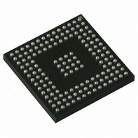
... The package of PI7C9X20404GP is a 12mm x 12mm LFBGA (148 Pin) package. The ball pitch is 0.8mm and the ball size is 0.5mm. The following are the package information and mechanical dimension: Figure 13-1 Bottom view drawing June 2009 – Revision 1.6 Pericom Semiconductor 4Port-4Lane PCI Express Switch Page PI7C9X20404GP ...
Page 78
... Figure 13-2 Package outline drawing June 2009 – Revision 1.6 Pericom Semiconductor 4Port-4Lane PCI Express Switch Page PI7C9X20404GP TM GreenPacket Family Datasheet ...
Page 79
... ORDERING INFORMATION Part Number □ PI7C9X20404GP NBE PI 7C 9X20404GP NB E June 2009 – Revision 1.6 Pericom Semiconductor Temperature Range Package 148-pin LFBGA (Industrial Temperature) 12mm x 12mm Blank=Standard E=Pb-Free and Green Package Code Blank=Standard =Revision Device Type Device Number Family PI=Pericom ...