SCANSTA101SM/NOPB National Semiconductor, SCANSTA101SM/NOPB Datasheet - Page 27
SCANSTA101SM/NOPB
Manufacturer Part Number
SCANSTA101SM/NOPB
Description
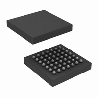
IC TEST MASTER LOW-VOLT 49FBGA
Manufacturer
National Semiconductor
Datasheet
1.SCANSTA101SMNOPB.pdf
(32 pages)
Specifications of SCANSTA101SM/NOPB
Applications
Testing Equipment
Interface
IEEE 1149.1
Voltage - Supply
3 V ~ 3.6 V
Package / Case
49-FBGA
Mounting Type
Surface Mount
Lead Free Status / RoHS Status
Lead free / RoHS Compliant
Other names
*SCANSTA101SM
*SCANSTA101SM/NOPB
SCANSTA101SM
*SCANSTA101SM/NOPB
SCANSTA101SM
Available stocks
Company
Part Number
Manufacturer
Quantity
Price
Company:

Part Number:
SCANSTA101SM/NOPB
Manufacturer:
Texas Instruments
Quantity:
10 000


16/32 bit Mode
TDO_SM Ctrl<11:10>
Sync Bit Length "x"
Default TDO Value
Debug Mode
ScanBridge Support Initiate/
Release
TRST
Reset
Test Loop-Back<1:0>
Bit(s)
14:10
11:10
9:7
1:0
15
6
5
4
3
2
'00'
'01'
'10'
'11'
'00'
'01'
'10'
'11'
'1'
'0'
'1'
'0'
'1'
'0'
'1'
'0'
'1'
'0'
'1'
'0'
Type
RW
RW
RW
RW
RW
RW
RW
RW
RW
RO
16/32 bit Mode
Reserved
TDO_SM Ctrl
Sync Bit Length
Default TDO Value
Debug Mode
ScanBridge Support Initiate/ Release
TRST
Reset
Test Loop-Back
Selects 16-bit or 32-bit external interface mode
32-bit external interface mode (used in macro form only)
16-bit external interface mode
TDO_SM Control bits
Hold previous value
Default TDO Value
Default TDO Value
High impedance
Sync Bit Length bits represents the number of sync bits to be used when the Sync Bit
Support Enable bit (17 in the Macro Structure) is set. The value "x" is the binary encoded
numeric value.
The value in this register will be sent out on the TDO_SM pin when performing a BIST or
a STATE Macro.
Drive TDO_SM to one.
Drive TDO_SM to zero.
Control bit to put SCANSTA101 in debug mode
Debug mode.
Normal mode.
ScanBridge support enable
Enable ScanBridge support
Disable ScanBridge support
Processor initiated ScanMaster test reset (on TRST0_SM and TRST1_SM_N). Bit is
cleared by a processor write.
Set TRST outputs low (active) and reset SSI logic.
Set TRST outputs high
Processor commanded synchronous reset to the serial scan logic for 2 clocks. This bit is
self clearing.
Reset the entire chip.
Release serial scan logic reset
Test loop-back mode bits
Normal operation
Loop-back TDO_SM to TDI_SM
Loop-back TMS_SM to TDI_SM
All Dot1 (1149.1) pins placed in SEU tolerant safe mode with: TMS_SM = 1, TCK_SM =
0, TDO_SM = Z, TRST0_SM = 0
TABLE 22. Setup Register (SETUPR) ($04)
Field
27
Address Offset
0
0
0
0
0
0
0
0
0
0
Reset Value
000b
00h
00b
11b
0b
1b
0b
0b
0b
0b
Reset Source
SYS_RST
SYS_RST
SYS_RST
SYS_RST
SYS_RST
SYS_RST
SYS_RST
SYS_RST
SYS_RST
www.national.com
Related parts for SCANSTA101SM/NOPB
Image
Part Number
Description
Manufacturer
Datasheet
Request
R

Part Number:
Description:
Low Voltage Ieee 1149.1 Sta Master
Manufacturer:
National Semiconductor Corporation
Datasheet:

Part Number:
Description:
National Semiconductor [8-Bit D/A Converter]
Manufacturer:
National Semiconductor
Datasheet:
Part Number:
Description:
National Semiconductor [Media Coprocessor]
Manufacturer:
National Semiconductor
Datasheet:
Part Number:
Description:
Digitally Controlled Tone and Volume Circuit with Stereo Audio Power Amplifier, Microphone Preamp Stage and National 3D Sound
Manufacturer:
National Semiconductor
Datasheet:
Part Number:
Description:
Digitally Controlled Tone and Volume Circuit with Stereo Audio Power Amplifier, Microphone Preamp Stage and National 3D Sound
Manufacturer:
National Semiconductor
Datasheet:
Part Number:
Description:
AC97 Rev 2 Codec with Sample Rate Conversion and National 3D Sound
Manufacturer:
National Semiconductor
Part Number:
Description:
Manufacturer:
National Semiconductor
Datasheet:
Part Number:
Description:
Manufacturer:
National Semiconductor
Datasheet:
Part Number:
Description:
General Purpose, Low Voltage, Low Power, Rail-to-Rail Output Operational Amplifiers
Manufacturer:
National Semiconductor
Datasheet:
Part Number:
Description:
8-bit 20 MSPS flash A/D converter.
Manufacturer:
National Semiconductor
Datasheet:
Part Number:
Description:
Low Noise Quad Operational Amplifier
Manufacturer:
National Semiconductor
Datasheet:
Part Number:
Description:
Quad Differential Line Receivers
Manufacturer:
National Semiconductor
Datasheet:
Part Number:
Description:
Quad High Speed Trapezoidal? Bus Transceiver
Manufacturer:
National Semiconductor
Datasheet:
Part Number:
Description:
Dual Line Receiver
Manufacturer:
National Semiconductor
Datasheet: