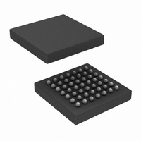
SCANSTA101SM/NOPB National Semiconductor, SCANSTA101SM/NOPB Datasheet - Page 10

SCANSTA101SM/NOPB
Manufacturer Part Number
SCANSTA101SM/NOPB
Description
IC TEST MASTER LOW-VOLT 49FBGA
Manufacturer
National Semiconductor
Datasheet
1.SCANSTA101SMNOPB.pdf
(32 pages)
Specifications of SCANSTA101SM/NOPB
Applications
Testing Equipment
Interface
IEEE 1149.1
Voltage - Supply
3 V ~ 3.6 V
Package / Case
49-FBGA
Mounting Type
Surface Mount
Lead Free Status / RoHS Status
Lead free / RoHS Compliant
Other names
*SCANSTA101SM
*SCANSTA101SM/NOPB
SCANSTA101SM
*SCANSTA101SM/NOPB
SCANSTA101SM
Available stocks
Company
Part Number
Manufacturer
Quantity
Price
Company:
Part Number:
SCANSTA101SM/NOPB
Manufacturer:
Texas Instruments
Quantity:
10 000
www.national.com
Bit 1
Bit 2
Module Descriptions
Figure 1
Parallel Processor Interface (PPI) and the Serial Scan Inter-
face (SSI) connect to each other through a dual-port memory.
The PPI provides a parallel interface for transferring data into
and out of the dual-port memory, and for configuring, control-
ling and obtaining the status of the device. The SSI, which
resides on the other side of the dual-port memory, provides
the parallel-to-serial and serial-to-parallel conversion paths
for providing test data and test control to support the STA
Master and IEEE 1532 functions.
Dual Port Memory
The Dual Port Memory module is a 2048 x 32 bit dual-port
memory which acts as the buffer between the PPI and the
0
0
1
1
0
0
0
0
1
1
1
1
0x3E0 - 0x3EF
0x3F0 - 0x3FF
0x7F0 - 0x7F7
0x7F8 - 0x7FF
0x00 - 0x1F
0x20 - 0x2F
0x30 - 0x3F
0x00 - 0x0F
0x10 - 0x17
0x18 - 0x1F
0x20 - 0x27
0x28 - 0x2F
..x.. - ..x..
..x.. - ..x..
shows a high level view of the SCANSTA101. The
Bit 0
Bit 1
Bit(s)
Bit(s)
0
1
0
1
0
0
1
1
0
0
1
1
Bit 0
Shift Macro with Capture
0
1
0
1
0
1
0
1
State Macro
BIST Macro
Shift Macro
Function
Ignore Headers and Trailers
Use Instruction Header
Use Instruction Trailer
Use both Instruction Header and Trailer
Use Data Header
Use Data Trailer
Use both Data Header and Trailer
Reserved
Function
Function
Sequence repeat count (up to 255)
Vector repeat count
Vector number
Repeat vector repeat count and vector number
Vector repeat count (up to 255)
Vector number (up to 63)
Function
Levels of Scan Bridge support to be inserted in the scan chain
Hierarchical Level 0 Scan Bridge Address
Hierarchical Level 0 Scan Bridge LSP
Hierarchical Level 1 Scan Bridge Address
Hierarchical Level 1 Scan Bridge LSP
Hierarchical Level Scan Bridge Address and LSP
Hierarchical Level 125 Scan Bridge Address
Hierarchical Level 125 Scan Bridge LSP
TABLE 11. Scan Bridge Support Structure
TABLE 9. Macro Type bits 10 and 11
TABLE 10. Sequencer Structure
TABLE 8. Header/Trailer Usage
Function
Loop on loop bit for Vector count. No Data
Loop on loop bit for vector count. Read data from TDO_SM memory
Loop on loop bit for vector count. Read data from TDO_SM memory
Do not loop on loop bit of macro. No data to be shifted
10
SSI. There are seven regions of memory as viewed from the
processor side. These regions, shown in
TDO_SM, TDI_SM, Expected, Mask, Vector, Header/Trailer,
Macro. Sequencer, and ScanBridge Support. Each has a
pointer which resides in the PPI.
The memory is big endian oriented and is viewed as a single
entity from the SSI side, and the SSI maintains a pointer. The
dual port memory module does not include any logic outside
of its own macro function, so all the timing and support logic
is included in the PPI and SSI sections. There is no logic in-
cluded in the SCANSTA101 design to utilize the "busy" indi-
cators to keep the user from overwriting memory locations.
The only area where this could occur in memory would be the
TDI_SM memory space since both the SSI and PPI can write
to this space, but the drivers should not allow PPI writes to
this area during normal operations. The National Semicon-
Table
4, are


