SCANSTA101SM/NOPB National Semiconductor, SCANSTA101SM/NOPB Datasheet
SCANSTA101SM/NOPB
Specifications of SCANSTA101SM/NOPB
*SCANSTA101SM/NOPB
SCANSTA101SM
Available stocks


Related parts for SCANSTA101SM/NOPB


SCANSTA101SM/NOPB Summary of contents
Page 1
... The SCANSTA101 is available as a stand-alone device pack- aged in a 49-pin BGA package also available macro for synthesis in programmable logic devices. SCANSTA101 Architecture TRI-STATE ® registered trademark of National Semiconductor Corporation. © 2010 National Semiconductor Corporation SCANSTA101 Features ■ Compatible with IEEE Std. 1149.1 (JTAG) Test Access Port and Boundary Scan Architecture ■ ...
Page 2
Figure 1 shows a high level view of the SCANSTA101 STA Master and its interfaces. Table 1 provides a brief description of each of these interfaces. Table 2 tion of the device pins and their functions. The device is composed ...
Page 3
TABLE 2. Pin Descriptions Pin Name No. Pins VCC GND D(15:0) D(31:16) (Note 1) A(4:0) SCK INT OE DTACK R/W STB CE RST TDO TDI TMS TCK TRST TDI_SM TDO_SM TMS_SM TCK_SM TRST0_SM TRST1_SM (Note 1) TRIST_SM Note 1: D(31:16) ...
Page 4
... Absolute Maximum Ratings If Military/Aerospace specified devices are required, please contact the National Semiconductor Sales Office/ Distributors for availability and specifications. Supply Voltage ( Input Diode Current ( −0. Input Voltage ( Output Diode Current ( −0. Output Voltage ( Output Source/Sink Current ( Ground Current CC per Output Pin ...
Page 5
AC Electrical Characteristics/Operating Requirements Over recommended operating supply voltage and temperature ranges unless otherwise specified. C otherwise specified. Symbol Parameter PARALLEL PROCESSOR INTERFACE (PPI) t Set Up Time S1 CE, R/W, Addr, Data to STB t Hold Time H1 CE, ...
Page 6
Symbol Parameter f Clock Frequency, SCK MAX t Release Time, RST to STB RELEASE Note 3: Due to uncertainty in the relationship of the STB placement to the system clock, SCK, the STB may be detected during the current or ...
Page 7
Symbol Parameter TEST & DEBUG INTERFACE TIMING REQUIREMENTS (SCAN) t Setup Time S TMS to TCK t Hold Time H TMS to TCK t Setup Time S TDI to TCK t Hold Time H TDI to TCK t Pulse Width ...
Page 8
Applications/Programmers Reference Address Type Mnemonic 00h RW START 01h RW STATUS 02h RW INTCTRL 03h RW INTSTAT 04h RW SETUPR 05h RW CLKDIV 07h RW EXPR 08h RW LSSEDR 09h RW MSSEDR 0Ah RW LSRESR 0Bh RW MSRESR 0Ch RW ...
Page 9
Function Macro Index Macro 1 Macro 2 Macro Macro Sequencer Index ...
Page 10
Bit 2 Bit 1 Bit 0 Function Ignore Headers and Trailers Use Instruction Header Use Instruction Trailer Use both Instruction Header and Trailer Use Data ...
Page 11
SCAN Ease software does not allow PPI writes to the TDI_SM memory. Parallel Processor Interface The overall function of the PPI is to receive the parallel data from the processor; store the data in the appropriate register or memory ...
Page 12
SSI also. A counter enable is passed from the SSI to indicate to the FG when the SSI's pointer value has changed decrement and an increment occur at the same time to either of the ...
Page 13
Figure 3, and the TDI_SM shifter block diagram is shown in Figure 4. Before the start of a vector processing the TMS_SM shifter is loaded with the least significant 16 bits of the macro structure. Based on the ...
Page 14
Reading from TDI_SM memory is accomplished by two con- secutive reads. When reading from the TDI_SM memory, the first read will contain the least significant 16 bits and the sec- ond read the most significant 16 bits. The TDI_SM shifter ...
Page 15
COMPARATOR AND EXPECTED/MASK REGISTERS The One-Bit Comparator, when enabled, compares the TDI_SM input with expected data. When the compare feature is enabled (in preloaded vector mode only) the SSIC pre- fetches data into Expected and Mask registers from the ad- ...
Page 16
The ScanBridge's TAP controller is then sequenced through the Update-DR state. E. Repeat Step 1C, but this time scan in the UNPARK instruction so that the LSP is inserted into the active scan chain. F. Sequence the ScanBridge's ...
Page 17
TDO buffer is empty, then gate TCK_SM until more data are available in the TDO buffer. When TCK_SM is disabled TMS_SM and TDO_SM will be driven with their previous values the Use Data/Instruction Trailer is enabled, fetch the ...
Page 18
FIGURE 8. Timing from Mode Register to Sequencer Start WRITING AND READING PARTIAL LONG WORDS Care should be taken when writing a partial long word to TDO_SM memory or reading a partial long word from TDI_SM memory. Since the TDO_SM ...
Page 19
TDO_SM IMPLEMENTATION The behavior of the TDO_SM output depends on the macro type that is being processed and the SETUP register bits 11 and 10, as shown in Table 13, regardless of the TAP tracker SETUP[11:10] TDO_SM 00 Hold Previous ...
Page 20
Signal Name No. of Pin Type Bits DTACK 1 O INT 1 O Signal Name No. Pin Type TDI_SM 1 I TDO_SM 1 O TMS_SM 1 O TCK_SM 1 O TRST0_SM 1 O TRST1_SM 1 O TRIST_SM 1 O www.national.com ...
Page 21
FIGURE 12. PPI Read Cycle Timing Diagram FIGURE 13. SSI Timing Diagram with Clock Divider set 10121538 10121539 www.national.com ...
Page 22
FIGURE 14. SSI Timing Diagram with Clock Divider set to 8 No. of Signal Name Pin Type Bits TDO 1 O TDI 1 I,U TMS 1 I,U TCK 1 I TRST 1 I,U,H SAFE MODE This device implements the following ...
Page 23
Software Interface Details REGISTER DEFINITIONS The following sections include descriptions of each address- able register in the ScanMaster memory space. Following the title of the particular register, the mnemonic for the register is Bit(s) Type 15:14 RO Reserved 13 RW ...
Page 24
Bit(s) Type 15 RW Results of Compare 14 RW BIST Running 13 RW Memory BIST Result 12 RW TDO Status Half-empty 11 RW TDO Status Empty 10 RW TDI Status Full 9 RW TDI Status Half-full 8 RW Using Sequencer ...
Page 25
TABLE 20. Interrupt Control Register (INTCTRL) ($02) Bit(s) Type 15:13 RO Reserved 12 RW TDO Half-empty Interrupt Enable 18 TDO Empty Interrupt Enable 10 RW TDI Full Interrupt Enable 9 RW TDI Half-full Interrupt Enable 8 RW Sequencer ...
Page 26
TABLE 21. Interrupt Status Register (INTSTAT) ($03) Bit(s) Type 15:13 RO Reserved 12 RW TDO Half-empty Interrupt 11 RW TDO Empty Interrupt 10 RW TDI Full Interrupt 9 RW TDI Half-full Interrupt 8 RW Sequencer Interrupt 7:3 RO Reserved Vector ...
Page 27
Bit(s) Type 15 RW 16/32 bit Mode 14:10 RO Reserved 11:10 RW TDO_SM Ctrl 9:7 RW Sync Bit Length 6 RW Default TDO Value 5 RW Debug Mode 4 RW ScanBridge Support Initiate/ Release 3 RW TRST 2 RW Reset ...
Page 28
Bit(s) Type 15:8 RO Reserved 7:1 RW Divisor 0 RO Reserved (hard coded) Note 23: LSB of the Clock Divider register is hard coded to zero. Divisor<7:1> '0000000' '0000001' '0000010' '0000100' '0001000' '0010000' '0100000' '1000000' TABLE 24. TDI_SM LFSR Exponent ...
Page 29
TABLE 28. TDI_SM LFSR MSB Result Register (MSRESR) ($0B) Bit(s) Type 15:0 RW MSW LFSR Result Note 30: MSW LFSR Result<15:0> is the MS word of the LFSR result. Note 31: This register along with register LSRESR form a register ...
Page 30
Testability Details - IEEE 1149.1 Support Instruction Mnemonic Binary Instruction Code EXTEST 000 SAMPLE/PRELOAD 001 BYPASS 111 IDCODE 010 HIGHZ 011 CLAMP 100 RUNBIST 110 SCANTEST 101 Version "0000" "1111 1100 0001 0111" BSR Signal Name BSR Bit# Bit# 0 ...
Page 31
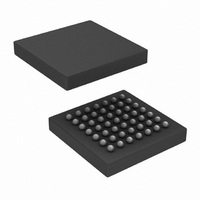
Physical Dimensions inches (millimeters) unless otherwise noted (Tape and Reel Ordering Code SCANSTA101SMX) 49-Pin BGA NS Package Number SLC49A Ordering Code SCANSTA101SM 31 www.national.com ...
Page 32
... For more National Semiconductor product information and proven design tools, visit the following Web sites at: www.national.com Products Amplifiers www.national.com/amplifiers Audio www.national.com/audio Clock and Timing www.national.com/timing Data Converters www.national.com/adc Interface www.national.com/interface LVDS www.national.com/lvds Power Management www.national.com/power Switching Regulators www.national.com/switchers LDOs www.national.com/ldo LED Lighting www ...