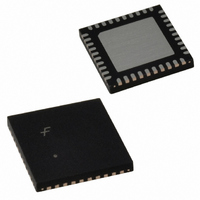
FIN24ACMLX Fairchild Semiconductor, FIN24ACMLX Datasheet - Page 5

FIN24ACMLX
Manufacturer Part Number
FIN24ACMLX
Description
IC SERIALIZER/DESERIALZR 40MLP
Manufacturer
Fairchild Semiconductor
Series
SerDes™r
Datasheet
1.FIN24ACMLX.pdf
(25 pages)
Specifications of FIN24ACMLX
Function
Serializer/Deserializer
Data Rate
520Mbps
Input Type
LVCMOS
Output Type
LVCMOS
Number Of Inputs
20
Number Of Outputs
20
Voltage - Supply
1.65 V ~ 3.6 V
Operating Temperature
-30°C ~ 70°C
Mounting Type
Surface Mount
Package / Case
40-MLP
Lead Free Status / RoHS Status
Lead free / RoHS Compliant
© 2005 Fairchild Semiconductor Corporation
FIN24AC Rev. 1.0.3
Control Logic Circuitry
The FIN24AC has the ability to be used as a 24-bit Seri-
alizer or a 24-bit Deserializer. Pins S1 and S2 must be
set to accommodate the clock reference input frequency
range of the serializer. Table 1 shows the pin program-
ming of these options based on the S1 and S2 control
pins. The DIRI pin controls whether the device is a serial-
izer or a deserializer. When DIRI is asserted LOW, the
device is configured as a deserializer. When the DIRI pin
is asserted HIGH, the device is configured as a serial-
izer. Changing the state on the DIRI signal reverses the
direction of the I/O signals and generates the opposite
state signal on DIRO. For unidirectional operation, the
DIRI pin should be hardwired to the HIGH or LOW state
and the DIRO pin should be left floating. For bi-
directional operation, the DIRI of the master device is
driven by the system and the DIRO signal of the master
is used to drive the DIRI of the slave device.
Serializer/Deserializer with Dedicated I/O
Variation
The serialization and deserialization circuitry is setup for
24 bits. Because of the dedicated inputs and outputs,
only 22 bits of data are ever serialized or deserialized.
Regardless of the mode of operation, the serializer is
always sending 24 bits of data and two boundary bits
and the deserializer is always receiving 24 bits of data
and two word boundary bits. Bits 23 and 24 of the serial-
izer always contain the value of zero and are discarded
by the deserializer. DP[21:22] input to the serializer is
deserialized to DP[23:24] respectively.
Table 1. Control Logic Circuitry
Number
Mode
0
1
2
3
S2
0
0
0
1
1
1
1
S1
0
1
1
0
0
1
1
DIRI
x
1
0
1
0
1
0
Power-Down Mode
24-Bit Serializer, 2MHz to 5MHz CKREF
24-Bit Deserializer
24-Bit Serializer, 5MHz to 15MHz CKREF
24-Bit Deserializer
24-Bit Serializer, 10MHz to 20MHz CKREF
24-Bit Deserializer
5
Turn-Around Functionality
The device passes and inverts the DIRI signal through
the device asynchronously to the DIRO signal. Care
must be taken during design to ensure that no contention
occurs between the deserializer outputs and the other
devices on this port. Optimally the peripheral device driv-
ing the serializer should be in a HIGH-impedance state
prior to the DIRI signal being asserted.
When a device with dedicated data outputs turns from a
deserializer to a serializer, the dedicated outputs remain
at the last logical value asserted. This value only changes
if the device is once again turned around into a deserial-
izer and the values are overwritten.
Power-Down Mode: (Mode 0)
Mode 0 is used for powering down and resetting the
device. When both of the mode signals are driven to a
LOW state, the PLL and references are disabled, differen-
tial input buffers are shut off, differential output buffers are
placed into a HIGH-impedance state, LVCMOS outputs
are placed into a HIGH-impedance state, LVCMOS
inputs are driven to a valid level internally, and all internal
circuitry is reset. The loss of CKREF state is also enabled
to ensure that the PLL only powers up if there is a valid
CKREF signal.
In a typical application, signals do not change states other
than between the desired frequency range and the power-
down mode. This allows for system-level power-down
functionality to be implemented via a single wire for a
SerDes pair. The S1 and S2 selection signals that have
their operating mode driven to a “logic 0” should be hard-
wired to GND. The S1 and S2 signals that have their
operating mode driven to a “logic 1” should be connected
to a system level power-down signal.
Description
www.fairchildsemi.com


