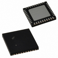
FIN24ACMLX Fairchild Semiconductor, FIN24ACMLX Datasheet - Page 16

FIN24ACMLX
Manufacturer Part Number
FIN24ACMLX
Description
IC SERIALIZER/DESERIALZR 40MLP
Manufacturer
Fairchild Semiconductor
Series
SerDes™r
Datasheet
1.FIN24ACMLX.pdf
(25 pages)
Specifications of FIN24ACMLX
Function
Serializer/Deserializer
Data Rate
520Mbps
Input Type
LVCMOS
Output Type
LVCMOS
Number Of Inputs
20
Number Of Outputs
20
Voltage - Supply
1.65 V ~ 3.6 V
Operating Temperature
-30°C ~ 70°C
Mounting Type
Surface Mount
Package / Case
40-MLP
Lead Free Status / RoHS Status
Lead free / RoHS Compliant
© 2005 Fairchild Semiconductor Corporation
FIN24AC Rev. 1.0.3
Notes:
4. Typical Values are given for V
5. Skew is measured form either the rising or falling edge of CKSO clock to the rising or falling edge of data (DSO).
6. The power-down time is a function of the CKREF frequency prior to CKREF being stopped HIGH or LOW and the
7. Signals are transmitted from the serializer source synchronously. In some cases, data is transmitted when the clock
8. Rising edge of CKP appears approximately 13 bit times after the falling edge of the CKP output. Falling edge of CKP
SERIALIZER AC ELECTRICAL CHARACTERISTICS
PLL AC ELECTRICAL CHARACTERISTICS
DESERIALIZER INPUT OPERATION CONDITIONS
DESERIALIZER AC ELECTRICAL CHARACTERISTICS
Symbol
t
t
t
TPLLS0
TPLLD0
TPLLD1
t
t
t
t
t
t
t
t
t
device and negative values refer to current flowing out of pins. Voltage is referenced to GROUND unless otherwise
specified (except ΔV
Signals are edge aligned. Both outputs should have identical load conditions for this test to be valid.
state of the S1/S2 mode pins. The specific number of clock cycles required for the PLL to be disabled varies based
on the operating mode of the device.
remains at a high state. Skew should only be measured when data and clock are transitioning at the same time. Total
measured input skew is a combination of output skew from the serializer, load variations, and ISI and jitter effects.
occurs approximately eight bit times after a data transition or six bit times after the falling edge of CKSO. Variation of
the data with respect of the CKP signal is due to internal propagation delay differences of the data and CKP path and
propagation delay differences on the various data pins. If the CKREF is not equal to STROBE for the serializer, the
CKP signal does not maintain a 50% duty cycle. The low time of CKP remains 13 bit times.
RCOP
RCOH
f
t
TCCD
SPOS
RCOL
t
ROLH
ROHL
t
f
S_DS
H_DS
MAX
HTC
PDV
STC
REF
Maximum Serial Data Rate
DP
DP
CKREF Frequency Relative to
Strobe Frequency
Transmitter Clock Input to
Clock Output Delay
CKSO Position Relative to DS See Figure 26
Serializer PLL Stabilization
Time
PLL Disable Time Loss of
Clock
PLL Power-Down Time
Serial Port Setup Time,
DS-to-CKSI
Serial Port Hold Time,
DS-to-CKS
Deserializer Clock Output
(CKP OUT) Period
CKP OUT Low Time
CKP OUT High Time
Data Valid to CKP LOW
Output Rise Time
(20% to 80%)
Output Fall Time
(80% to 20%)
(n)
(n)
Setup to STROBE
Hold to STROBE
Parameter
OD
and V
OD
DD
).
= 2.775V and T
CKREF x 26
DIRI = 1
See Figure 9 (f = 5MHz)
CKREF Does Not Equal STROBE
See Figure 23, DIRI = 1,
CKREF = STROBE
See Figure 22
See Figure 27
See Figure 28
See Figure 25
See Figure 25
See Figure 21
See Figure 21 (Rising Edge Strobe)
Serializer Source STROBE = CKREF
where a = (1 /f ) / 26
See Figure 21 (Rising Edge Strobe)
where a = (1 /f ) / 26
C
L
= 5pF, See Figure 18
Test Conditions
A
= 25°C. Positive current values refer to the current flowing into
(5)
(6)
(7)
(7)
16
(8)
(8)
S2 = 1 S1 = 0
S2 = 1 S1 = 1
S2 = 0 S1 = 1
33a + 1.5
f
STROBE
13a-3
13a-3
–50.0
Min.
1.1 x
–250
52.0
50.0
8a-6
130
260
2.5
2.0
1.4
Typ.
2.5
2.5
T
(4)
35a + 6.5
13a+3
13a+3
Max.
8a+1
20.0
30.0
20.0
130
390
520
250
200
500
www.fairchildsemi.com
Units
Mb/s
MHz
ns
ns
ns
ps
µs
µs
ns
ns
ps
ns
ns
ns
ns
ns
ns


