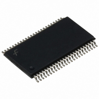
FIN1217MTDX Fairchild Semiconductor, FIN1217MTDX Datasheet - Page 12

FIN1217MTDX
Manufacturer Part Number
FIN1217MTDX
Description
IC SERIALIZER/DESERIAL 48-TSSOP
Manufacturer
Fairchild Semiconductor
Type
LVDS 21-Bit Serializer/Deserializerr
Datasheet
1.FIN1215MTDX.pdf
(20 pages)
Specifications of FIN1217MTDX
Function
Serializer/Deserializer
Data Rate
1.785Gbps
Input Type
LVTTL
Output Type
LVDS
Number Of Inputs
21
Number Of Outputs
3
Voltage - Supply
3 V ~ 3.6 V
Operating Temperature
-40°C ~ 85°C
Mounting Type
Surface Mount
Package / Case
48-TSSOP
Number Of Drivers
3
Number Of Receivers
21
Operating Supply Voltage
3.3 V
Maximum Operating Temperature
+ 150 C
Minimum Operating Temperature
- 65 C
Mounting Style
SMD/SMT
Supply Current
55 mA
Supply Voltage (max)
3.6 V
Supply Voltage (min)
3 V
Lead Free Status / RoHS Status
Lead free / RoHS Compliant
Other names
FIN1217MTDX
FIN1217MTDXTR
FIN1217MTDXTR
© 2003 Fairchild Semiconductor Corporation
FIN1215 / FIN1216 / FIN1217 • Rev. 1.0.3
Receiver AC Electrical Characteristics
Notes:
16. Total channel latency from serializer to deserializer is (T + t
17. Receiver skew margin is defined as the valid sampling window after considering potential setup/hold time and
Symbol
t
t
t
t
t
t
t
t
t
t
t
t
t
t
t
t
minimum/maximum bit position.
RSPB0
RSPB1
RSPB2
RSPB3
RSPB4
RSPB5
RSPB6
RSPB0
RSPB1
RSPB2
RSPB3
RSPB4
RSPB5
RSPB6
RPLLS
RSKM
Receiver Input Strobe Position of Bit 0
Receiver Input Strobe Position of Bit 1
Receiver Input Strobe Position of Bit 2
Receiver Input Strobe Position of Bit 3
Receiver Input Strobe Position of Bit 4
Receiver Input Strobe Position of Bit 5
Receiver Input Strobe Position of Bit 6
Receiver Input Strobe Position of Bit 0
Receiver Input Strobe Position of Bit 1
Receiver Input Strobe Position of Bit 2
Receiver Input Strobe Position of Bit 3
Receiver Input Strobe Position of Bit 4
Receiver Input Strobe Position of Bit 5
Receiver Input Strobe Position of Bit 6
RxIn Skew Margin
found.)
Receiver Phase Lock Loop Set Time
Parameter
(Error! Reference source not
(Continued)
12
Figure 21
f=65MHz
Figure 21
f=85MHz
FIN1218 only
f=40MHz, Figure 22
f=65MHz, Figure 22
f=85MHz
FIN1218 only
Figure 22
Figure 16
Conditions
TCCD
) + (2•T + t
RCCD
10.57
).
Min.
11.7
13.9
0.49
2.17
3.85
5.53
7.21
8.89
490
400
252
0.7
2.9
5.1
7.3
9.5
Typ.
Max.
11.27
10.2
12.4
14.6
1.19
2.87
4.55
6.23
7.91
9.59
10.0
1.4
3.6
5.8
8.0
www.fairchildsemi.com
Units
ms
ns
ns
ns
ns
ns
ns
ns
ns
ns
ns
ns
ns
ns
ns
ps


