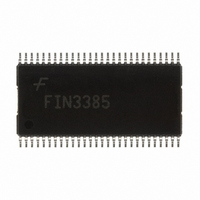
FIN3385MTDX Fairchild Semiconductor, FIN3385MTDX Datasheet - Page 15

FIN3385MTDX
Manufacturer Part Number
FIN3385MTDX
Description
IC SERIALIZER/DESERIAL 56-TSSOP
Manufacturer
Fairchild Semiconductor
Type
Low Voltage 28-Bit Flat Panel Display Linkr
Datasheet
1.FIN3384MTDX.pdf
(21 pages)
Specifications of FIN3385MTDX
Function
Serializer/Deserializer
Data Rate
2.38Gbps
Input Type
LVTTL
Output Type
LVDS
Number Of Inputs
28
Number Of Outputs
4
Voltage - Supply
3 V ~ 3.6 V
Operating Temperature
-10°C ~ 70°C
Mounting Type
Surface Mount
Package / Case
56-TSSOP
Ic Output Type
LVDS
No. Of Inputs
28
No. Of Outputs
4
Supply Voltage Range
3V To 3.6V
Driver Case Style
TSSOP
No. Of Pins
56
Termination Type
SMD
Rohs Compliant
Yes
Number Of Drivers
4
Number Of Receivers
28
Operating Supply Voltage
3.3 V
Maximum Operating Temperature
+ 150 C
Minimum Operating Temperature
- 65 C
Mounting Style
SMD/SMT
Supply Current
41.8 mA
Supply Voltage (max)
3.6 V
Supply Voltage (min)
3 V
Filter Terminals
SMD
Digital Ic Case Style
TSSOP
Lead Free Status / RoHS Status
Lead free / RoHS Compliant
Other names
FIN3385MTDX
FIN3385MTDXTR
FIN3385MTDXTR
© 2003 Fairchild Semiconductor Corporation
FIN3383/3384/3385/3386 • Rev. 1.0.4
Note:
AC Loadings and Waveforms
22. For the receiver with falling-edge strobe, the definition of setup/hold time is slightly different from the one with
rising-edge strobe. The clock reference point is the time when the clock falling edge passes through 2V. For
hold time t
RHRC
Figure 13. Transmitter Clock-In to Clock-Out Delay (Rising-Edge Strobe)
, the clock reference point is the time when falling edge passes through +0.8V.
Figure 14. Receiver Clock-In to Clock-Out Delay (Falling-Edge Strobe)
Figure 12. Receiver Setup/Hold and HIGH/LOW Times
Figure 15. Receiver Phase Lock Loop Set Time
(Continued)
15
www.fairchildsemi.com


