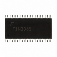
FIN3385MTDX Fairchild Semiconductor, FIN3385MTDX Datasheet - Page 11

FIN3385MTDX
Manufacturer Part Number
FIN3385MTDX
Description
IC SERIALIZER/DESERIAL 56-TSSOP
Manufacturer
Fairchild Semiconductor
Type
Low Voltage 28-Bit Flat Panel Display Linkr
Datasheet
1.FIN3384MTDX.pdf
(21 pages)
Specifications of FIN3385MTDX
Function
Serializer/Deserializer
Data Rate
2.38Gbps
Input Type
LVTTL
Output Type
LVDS
Number Of Inputs
28
Number Of Outputs
4
Voltage - Supply
3 V ~ 3.6 V
Operating Temperature
-10°C ~ 70°C
Mounting Type
Surface Mount
Package / Case
56-TSSOP
Ic Output Type
LVDS
No. Of Inputs
28
No. Of Outputs
4
Supply Voltage Range
3V To 3.6V
Driver Case Style
TSSOP
No. Of Pins
56
Termination Type
SMD
Rohs Compliant
Yes
Number Of Drivers
4
Number Of Receivers
28
Operating Supply Voltage
3.3 V
Maximum Operating Temperature
+ 150 C
Minimum Operating Temperature
- 65 C
Mounting Style
SMD/SMT
Supply Current
41.8 mA
Supply Voltage (max)
3.6 V
Supply Voltage (min)
3 V
Filter Terminals
SMD
Digital Ic Case Style
TSSOP
Lead Free Status / RoHS Status
Lead free / RoHS Compliant
Other names
FIN3385MTDX
FIN3385MTDXTR
FIN3385MTDXTR
© 2003 Fairchild Semiconductor Corporation
FIN3383/3384/3385/3386 • Rev. 1.0.4
Receiver DC Electrical Characteristics
Typical values are at T
temperatures ranges, unless otherwise specified.
Notes:
Symbol
15. The power supply current for the receiver can be different with the number of I/O channels.
16. Total channel latency from serializer to deserializer is (T + t
17. Receiver skew margin is defined as the valid sampling window after considering potential setup/hold time and
t
t
t
t
t
t
t
t
t
t
t
t
t
t
t
t
t
t
RSPB0
RSPB1
RSPB2
RSPB3
RSPB4
RSPB5
RSPB6
RPLLS
RCOH
RCOP
RCOL
RSRC
RHRC
ROLH
ROHL
RCCD
RPPD
RSKM
minimum/maximum bit position.
Receiver Clock Output (RxCLKOut)
Period
RxCLKOut LOW Time
RxCLKOut HIGH Time
RxOut Valid Prior to RxCLKOut
RxOut Valid After RxCLKOut
Output Rise Time (20% to 80%)
Output Rise Time (80% to 20%)
Receiver Clock Input to Clock Output
Delay
Receiver Power-Down Delay
Receiver Input Strobe Position of Bit 0
Receiver Input Strobe Position of Bit 1
Receiver Input Strobe Position of Bit 2
Receiver Input Strobe Position of Bit 3
Receiver Input Strobe Position of Bit 4
Receiver Input Strobe Position of Bit 5
Receiver Input Strobe Position of Bit 6
RxIN Skew Margin
Receiver Phase Lock Loop Set Time
(16)
A
=25°C and with V
Parameter
(17)
CC
=3.3V; minimum and maximum are at over supply voltages and operating
(Continued)
11
Figure 12
Rising Edge Strobe
f=85MHz
C
T
V
Figure 24
Figure 17
Figure 21
f=85MHz
Figure 21
Figure 21
A
L
CC
=25°C and
=8pF, Figure 8
=3.3V
Conditions
TCCD
). There is a clock period.
11.76
10.57
Min.
0.49
2.17
3.85
5.53
7.21
8.89
290
4.0
4.5
3.5
3.5
3.5
10.92
Typ.
0.84
2.52
4.20
5.88
7.56
9.24
5.0
5.0
2.0
1.8
5.0
10
T
Max.
50.00
11.27
1.19
2.87
4.55
6.23
7.91
9.59
6.0
6.5
3.5
3.5
7.5
1.0
www.fairchildsemi.com
Units
ms
ns
ns
ns
ns
ns
ns
µs
ns
ns
ns
ns
ns
ns
ns
ps


