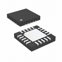
LTC6601CUF-2#TRPBF Linear Technology, LTC6601CUF-2#TRPBF Datasheet - Page 6

LTC6601CUF-2#TRPBF
Manufacturer Part Number
LTC6601CUF-2#TRPBF
Description
IC FILTER/ADC DVR LP LD 20-QFN
Manufacturer
Linear Technology
Datasheet
1.LTC6601CUF-2PBF.pdf
(40 pages)
Specifications of LTC6601CUF-2#TRPBF
Frequency - Cutoff Or Center
27MHz
Number Of Filters
3
Max-order
2nd
Voltage - Supply
2.7 V ~ 5.25 V
Mounting Type
Surface Mount
Package / Case
20-QFN
Lead Free Status / RoHS Status
Lead free / RoHS Compliant
Filter Type
-
Available stocks
Company
Part Number
Manufacturer
Quantity
Price
Part Number:
LTC6601CUF-2#TRPBFLTC6601CUF-2#PBF
Manufacturer:
Linear Technology
Quantity:
135
ELECTRICAL CHARACTERISTICS
LTC6601-2
Note 1: Stresses beyond those listed under the Absolute Maximum
Ratings may cause permanent damage to the device. Exposure to any
Absolute Maximum Rating condition for extended periods may affect
device reliability and lifetime.
Note 2: All pins are protected by steering diodes to either supply. If any
pin is driven beyond the part’s supply voltage, the excess input current
(current in excess of what it takes to drive that pin to the supply rail)
should be limited to less than 10mA.
Note 3: A heat sink may be required to keep the junction temperature
below the Absolute Maximum Rating when the output is shorted
indefi nitely. Long-term application of output currents in excess of the
Absolute Maximum Ratings may impair the life of the device.
Note 4: The LTC6601C/LTC6601I are guaranteed functional over the
operating temperature range –40°C to 85°C.
Note 5: The LTC6601C is guaranteed to meet specifi ed performance from
0°C to 70°C. The LTC6601C is designed, characterized, and expected
to meet specifi ed performance from –40°C to 85°C but is not tested or
QA sampled at these temperatures. The LTC6601I is guaranteed to meet
specifi ed performance from –40°C to 85°C.
Note 6: Output referred voltage offset is a function of the low frequency
gain of the LTC6601. To determine output referred voltage offset, or output
voltage offset drift, multiply this specifi cation by the noise gain (1 + GAIN).
See Applications Information for more details.
Note 7: Input bias current is defi ned as the average of the currents
fl owing into the noninverting and inverting inputs of the internal amplifi er
and is calculated from measurements made at the pins of the IC. Input
offset current is defi ned as the difference of the currents fl owing into the
noninverting and inverting inputs of the internal amplifi er and is calculated
from measurements made at the pins of the IC.
Note 8: Input common mode range is tested using the test circuit of
Figure 1 by measuring the differential DC gain with V
with V
Characteristics table, verifying the differential gain has not deviated from
6
ICM
at the input common mode range limits listed in the Electrical
ICM
= mid-supply, and
the mid-supply common mode input case by more than 1%, and the
common mode offset (V
common mode offset by more than ±20mV.
The voltage range for the output common mode range is tested using the
test circuit of Figure 1 by measuring the differential DC gain with V
mid-supply, and again with a voltage set on the V
Characteristics table limits, checking the differential gain has not deviated
from the mid-supply common mode input case by more than 1%, and that
the common mode offset (V
from the mid-supply case.
Note 9: Input CMRR is defi ned as the ratio of the change in the input
common mode voltage at the amplifi er input to the change in differential
input referred voltage offset. Output CMRR is defi ned as the ratio of the
change in the voltage at the V
referred voltage offset.
Note 10: Power supply rejection (PSRR) is defi ned as the ratio of the
change in supply voltage to the change in differential input referred voltage
offset. Common mode power supply rejection (PSRRCM) is defi ned as the
ratio of the change in supply voltage to the change in the common mode
offset, V
Note 11: Output swings are measured as differences between the output
and the respective power supply rail.
Note 12: Extended operation with the output shorted may cause junction
temperatures to exceed the 150°C limit and is not recommended.
Note 13: Floating the BIAS pin will reliably place the part into the half-
power mode. The pin does not have to be driven. Care should be taken,
however, to prevent external leakage currents in or out of this pin from
pulling the pin into an undesired state.
Note 14: The variable contact resistance of the high speed test equipment
limits the accuracy of this test. These parameters only show a typical
value, or conservative minimum and maximum value.
OUTCM
/V
OCM
.
OCMOS
OCMOS
OCM
) has not deviated from the mid-supply
pin to the change in differential input
) has not deviated by more than ±20mV
OCM
pin at the Electrical
OCM
66012f
=


